LTC1798CS8-2.5-TRPBF データシートの表示(PDF) - Linear Technology
部品番号
コンポーネント説明
メーカー
LTC1798CS8-2.5-TRPBF Datasheet PDF : 10 Pages
| |||
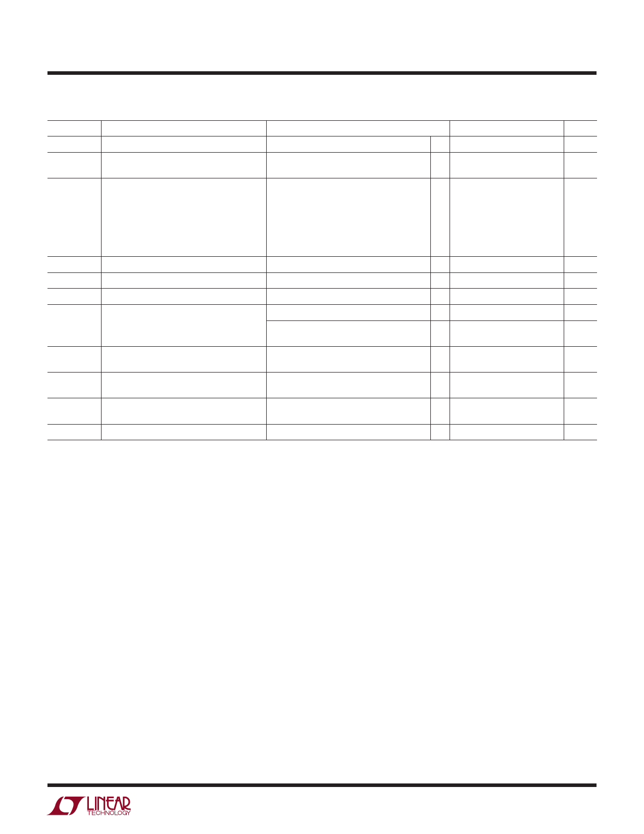
LTC1798 Series
ELECTRICAL CHARACTERISTICS The l denotes specifications which apply over the full specified temperature
range, otherwise specifications are at TA = 25°C. VIN = VOUT(NOMINAL) + 0.2V, IOUT = 0mA unless otherwise noted. FB = OUT for the LTC1798.
SYMBOL
PARAMETER
CONDITIONS
MIN TYP MAX UNITS
VIN
Input Voltage Range
l
12.6
V
IIN
Input Current
FB = OUT for LTC1798
4
6.5
µA
l
8.5
µA
VOUT
Output Voltage (Note 4)
LTC1798, FB = OUT
LTC1798 ADJ
LTC1798-2.5
LTC1798-3
LTC1798-4.1
LTC1798-5
LTC1798 All Fixed Options
2.3755 2.385 2.3945
V
–0.4
0.4
%
2.4963 2.5 2.5037
V
2.9955 3 3.0045
V
4.090 4.096 4.102
V
4.9925 5 5.0075
V
–0.15
0.15
%
en
Output Voltage Noise (Note 5)
0.1Hz ≤ f ≤ 10Hz
8
ppmP-P
TC
Output Voltage Temp Coefficient (Note 6) TMIN ≤ TJ ≤ TMAX
l
15
40 ppm/°C
VOUT/VIN
VOUT/IOUT
Line Regulation
Load Regulation (Note 7)
VIN = (VOUT(NOMINAL) + 0.2V) to 12.6V
l
Sourcing 0mA to 10mA
l
Sinking 0mA to 2mA
l
30
120 ppm/V
0.1
0.3 mV/mA
1.75
4 mV/mA
6.5 mV/mA
ISC
∆VDO
VHYST
Short-Circuit Output Current
Dropout Voltage (Note 8)
Output Hysteresis (Note 9)
VOUT Shorted to GND
VOUT Shorted to VIN
IOUT = 0, ∆VOUT ≤ 0.1%
IOUT = 10mA, ∆VOUT ≤ 0.1%
∆T = –40°C to 85°C
∆T = 0°C to 70°C
20
40
mA
2
4
mA
l
100
mV
l
200
mV
200
ppm
50
ppm
IFB
FB Pin Input Current
LTC1798, OUT = FB
10
nA
Note 1: Stresses beyond those listed under Absolute Maximum Ratings
may cause permanent damage to the device. Exposure to any Absolute
Maximum Rating condition for extended periods may affect device
reliability and lifetime.
Note 2: The LTC1798 is guaranteed functional over the operating
temperature range of –40°C to 100°C.
Note 3: If the part is stored outside of the specified operating temperature
range, the output may shift due to hysteresis.
Note 4: ESD (Electostatic Discharge) sensitive device. Extensive use of
ESD protection devices are used internal to the LTC1798, however, high
electrostatic discharge can damage or degrade the device. Use proper ESD
handling precautions.
Note 5: Peak-to-peak noise is measured with a single pole highpass filter
at 0.1Hz and 2-pole lowpass filter at 10Hz.
Note 6: Temperature coefficient is the change in output voltage divided by
the nominal output voltage divided by the specified temperature range.
Note 7: Load regulation is measured on a pulse basis from no load to the
specified load current. Output changes due to die temperature change
must be taken into account separately.
Note 8: Dropout voltage is (VIN – VOUT) when VOUT falls to 0.1% below its
nominal value at VIN = VOUT + 0.5V.
Note 9: Hysteresis in output voltage is created by package stress that
differs depending on whether the IC was previously at a higher or lower
temperature. Output voltage is always measured at 25°C, but the IC is
cycled hot or cold before successive measurements. Hysteresis is not
normally a problem for operational temperature excursions where the
instrument might be stored at high or low temperature.
1798fc
3
Share Link: 