LTC2050HS6 データシートの表示(PDF) - Linear Technology
部品番号
コンポーネント説明
メーカー
LTC2050HS6 Datasheet PDF : 16 Pages
| |||
LTC2050/LTC2050HV
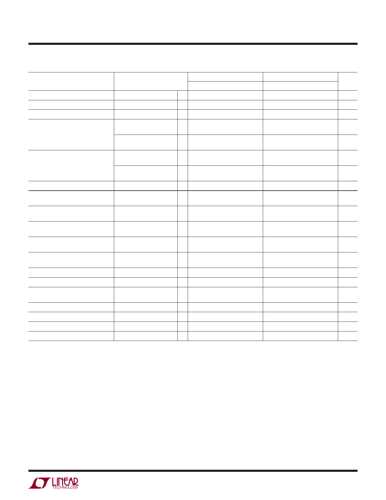
ELECTRICAL CHARACTERISTICS The l denotes the specifications which apply over the full operating
temperature range, otherwise specifications are at TA = 25°C. (LTC2050, LTC2050HV) VS = 5V unless otherwise noted. (Note 3)
C, I SUFFIXES
H SUFFIX
PARAMETER
CONDITIONS
MIN
TYP
MAX
MIN
TYP
MAX UNITS
Input Offset Voltage
(Note 2)
±0.5
±3
±0.5
±3
μV
Average Input Offset Drift
Long-Term Offset Drift
(Note 2)
l
±0.03
50
±0.05 μV/°C
50
nV/√mo
Input Bias Current
LTC2050
±75
±150
l
±300
±75
±150
pA
±4000
pA
LTC2050HV
±7
±50
l
±150
±7
±50
pA
±4000
pA
Input Offset Current
LTC2050
±300
l
±400
±300
pA
±1000
pA
LTC2050HV
±100
l
±200
±100
pA
±1000
pA
Input Noise Voltage
Common Mode Rejection Ratio
Power Supply Rejection Ratio
RS = 100Ω, 0.01Hz to 10Hz
1.5
VCM = GND to (V+ – 1.3)
120
130
VCM = GND to (V+ – 1.3)
l 115
130
VS = 2.7V to 6V
120
130
l 115
130
1.5
120
130
110
130
120
130
115
130
μVP-P
dB
dB
dB
dB
Large-Signal Voltage Gain
RL = 10k
125
140
125
140
dB
l 120
140
115
140
dB
Output Voltage Swing High
Output Voltage Swing Low
Slew Rate
RL = 2k to GND
RL = 10k to GND
RL = 2k to GND
RL = 10k to GND
l 4.85
4.94
4.85
4.94
V
l 4.95
4.98
4.95
4.98
V
l
1
10
l
1
10
1
10
mV
1
10
mV
2
2
V/μs
Gain Bandwidth Product
3
3
MHz
Supply Current
Shutdown Pin Input Low Voltage (VIL)
Shutdown Pin Input High Voltage (VIH)
Shutdown Pin Input Current
VSHDN = VIH, No Load
VSHDN = VIL
VSHDN = GND
l
0.8
1.2
l
15
0.8
1.3
mA
15
μA
l
V– + 0.5
V– + 0.5
V
l V+ – 0.5
V+ – 0.5
V
l
–0.5
–7
–0.5
–7
μA
Internal Sampling Frequency
7.5
7.5
kHz
2050fb
5
Share Link: 