LTC2904 データシートの表示(PDF) - Linear Technology
部品番号
コンポーネント説明
メーカー
LTC2904 Datasheet PDF : 16 Pages
| |||
LTC2904/LTC2905
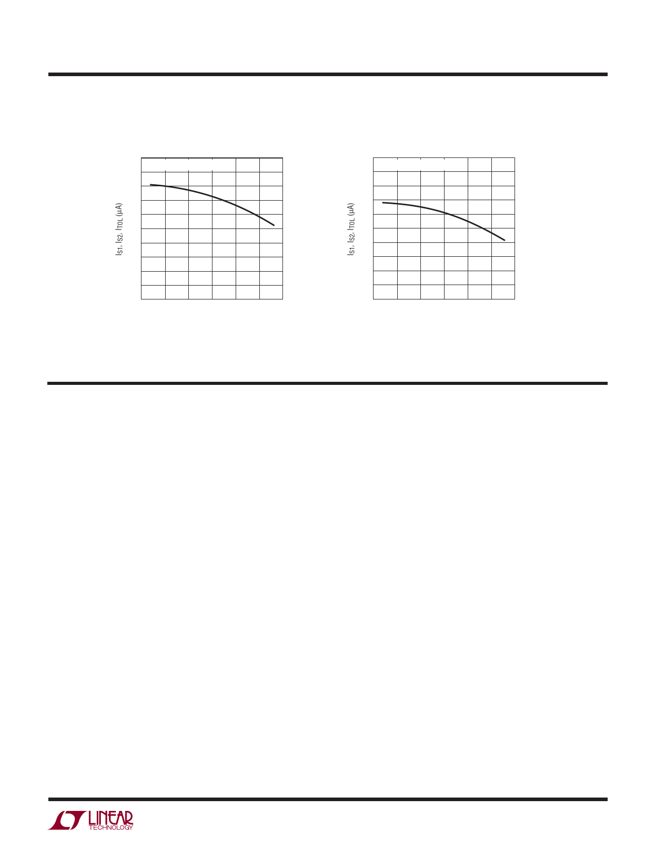
TYPICAL PERFORMANCE CHARACTERISTICS
Specifications are at TA = 25°C unless otherwise noted.
IS1, IS2, ITOL vs Temperature
20
S1 = S2 = TOL = 3.3V
19
18
17
16
15
14
13
12
11
10
–50 –25 0 25 50 75 100
TEMPERATURE (oC)
29045 G25
IS1, IS2, ITOL vs Temperature
–20
S1 = S2 = TOL = GND
–19
–18
–17
–16
–15
–14
–13
–12
–11
–10
–50 –25 0 25 50 75 100
TEMPERATURE (oC)
29045 G26
PIN FUNCTIONS (TS8/DDB8)
V2 (Pin 1/Pin 4): Voltage Input 2. Input for V2 monitor.
Select from 3.3V, 2.5V, 1.8V, 1.5V, 1.2V or 1.0V. Refer to
Table 1 for details. The greater of V1, V2 is also the internal
supply voltage, VCC. Bypass this pin to ground with a 0.1μF
(or greater) capacitor.
RST (Pin 2/Pin 3): (LTC2904 Only) Reset Logic Output.
When all voltage inputs are above the reset threshold for
at least the programmed delay time, this pin pulls low. This
pin has a weak pull-up to VCC and may be pulled above
VCC using an external pull-up.
TMR (Pin 2/Pin 3): (LTC2905 Only) Reset Delay Time
Programming Pin. Attach an external capacitor (CTMR) to
GND to set a reset delay time of 9ms/nF. Leaving the pin
open generates a minimum delay of approximately 200μs. A
22nF capacitor will generate a 200ms reset delay time.
RST (Pin 3/Pin 2): Inverted Reset Logic Output. Pulls low
when any voltage input is below the reset threshold and is
held low for programmed delay time after all voltage inputs
are above threshold. This pin has a weak pull-up to VCC
and may be pulled above VCC using an external pull-up.
GND (Pin 4/Pin 1, Pin 9): Ground.
TOL (Pin 5/Pin 8): Three-state Input for Supply Tolerance
Selection (5%, 7.5% or 10%). See the Applications Infor-
mation section for tolerance selection chart (Table 2).
S1 (Pin 6/Pin 7): Voltage Threshold Select Three-State
Input. Connect to V1, GND or leave unconnected in open
state (See Table 1).
S2 (Pin 7/Pin 6): The Second Voltage Threshold Select
Three-State Input. Connect to V1, GND or leave uncon-
nected in open state (See Table 1).
V1 (Pin 8/Pin 5): Voltage Input 1. Input for V1 monitor.
Select from 5V, 3.3V, or 2.5V. See Table 1 for details.
The greater of V1, V2 is also the internal supply voltage,
VCC. Bypass this pin to ground with a 0.1μF (or greater)
capacitor.
29045fd
7
Share Link: 