LTC2906 データシートの表示(PDF) - Linear Technology
部品番号
コンポーネント説明
メーカー
LTC2906
Linear Technology

LTC2906 Datasheet PDF : 16 Pages
| |||
LTC2906/LTC2907
APPLICATIO S I FOR ATIO
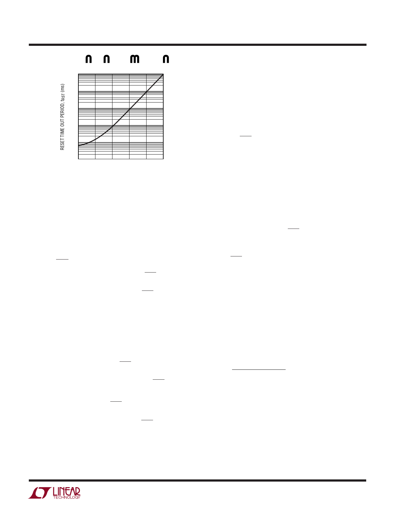
10000
1000
100
Note however, by adding an external pull-up resistor, the
pull-up strength on the RST pin is increased. Therefore, if
it is connected in a wired-OR connection, the pull-down
strength of any single device needs to accommodate this
additional pull-up strength.
10
1
0.1
10p 100p 1n
10n 100n 1µ
CTMR (FARAD)
29067 F02
Figure 2. Reset Time-Out Period vs Capacitance
Leaving the TMR pin open with no external capacitor
generates a reset time-out of approximately 200µs. For
long reset time-out, the only limitation is the availability of
a large value capacitor with low leakage. The TMR capaci-
tor will never charge if the leakage current exceeds the
TMR charging current of 2.1µA (typical).
RST and RST Output Characteristics
The DC characteristics of the RST and RST pull-up and
pull-down strength are shown in the Typical Performance
Characteristics section. Both RST and RST have a weak
internal pull-up to VMAX and a strong pull-down to ground.
The weak pull-up and strong pull-down arrangement
allows these two pins to have open-drain behavior while
possessing several other beneficial characteristics.
The weak pull-ups eliminate the need for external pull-up
resistors when the rise time on these pins is not critical. On
the other hand, the open-drain RST configuration allows
for wired-OR connections and can be useful when more
than one signal needs to pull-down on the RST line.
As noted in the Power-Up and Power-Down sections, the
circuits that drive RST and RST are powered by VMAX =
MAX (V1, VCC). During fault condition, VMAX of at least 1V
guarantees a maximum VOL = 0.4V at RST. However, at
VMAX = 1V the weak pull-up current on RST is barely turned
on. Therefore, an external pull-up resistor of no more than
100k is recommended on the RST pin if the state and pull-
up strength of the RST pin is crucial at very low VMAX.
Output Rise and Fall Time Estimation
The RST and RST output have strong pull-down capability.
The following formula estimates the output fall time (90%
to 10%) for a particular external load capacitance (CLOAD):
tFALL ≈ 2.2␣ •␣ RPD␣ •␣ CLOAD
where RPD is the on-resistance of the internal pull-down
transistor estimated to be typically 40Ω at VMAX >1V, at
room temperature (25°C), and CLOAD is the external load
capacitance on the pin. Assuming a 150pF load capaci-
tance, the fall time is about 13ns.
The rise time on the RST and RST pins is limited by weak
internal pull-up current sources to VMAX. The following
formula estimates the output rise time (10% to 90%) at the
RST and RST pins:
tRISE ≈ 2.2 • RPU • CLOAD
where RPU is the on-resistance of the pull-up transistor.
Notice that this pull-up transistor is modeled as a
6µA current source in the Block Diagram as a typical
representation.
The on-resistance as a function of the VMAX = MAX (V1,
VCC) voltage (for VMAX > 1V) at room temperature is
estimated as follows:
RPU
=
6 •105
MAX(V1, VCC) –
1V
Ω
At VMAX = 3.3V, RPU is about 260k. Using 150pF for load
capacitance, the rise time is 86µs. A smaller external pull-
up resistor maybe used if the output needs to pull up faster
and/or to a higher voltage. For example, the rise time
reduces to 3.3µs for a 150pF load capacitance, when using
a 10k pull-up resistor.
29067f
11
Share Link: