LTC2909(RevA) データシートの表示(PDF) - Linear Technology
部品番号
コンポーネント説明
メーカー
LTC2909 Datasheet PDF : 16 Pages
| |||
LTC2909
APPLICATIO S I FOR ATIO
The above discussion is concerned only with the DC
value of the monitored supply. Real supplies also have
relatively high frequency variation from sources such as
load transients, noise and pickup. These variations should
not be considered by the monitor in determining whether
a supply voltage is valid or not. The variations may cause
spurious outputs at ⎯R⎯S⎯T, particularly if the supply voltage
is near its trip threshold.
A common solution to the problem of spurious reset is
to introduce hysteresis around the nominal threshold.
However, this hysteresis degrades the effective accuracy
of the monitor and increases the range over which the
system must operate. The LTC2909 therefore does not
have hysteresis, except in comparator mode (see Setting
the Reset Timeout). If hysteresis is desired in other modes,
it may be added externally. See Typical Applications for
an example.
The LTC2909 uses two techniques to combat spurious
reset without sacrificing threshold accuracy. First, the
timeout period helps prevent high frequency variation
whose frequency is above 1/ tRST from appearing at the
⎯R⎯S⎯T output.
When either ADJ1 or ADJ2 becomes invalid, the ⎯R⎯S⎯T pin
asserts low. When the supply recovers past the threshold,
the reset timer starts (assuming it is not disabled) and ⎯R⎯S⎯T
does not go high until it finishes. If the supply becomes
invalid any time during the timeout period, the timer resets
and starts fresh when the supply next becomes valid.
While the reset timeout is useful at preventing toggling of
the reset output in most cases, it is not effective at pre-
venting nuisance resets due to short glitches (from load
transients or other effects) on a valid supply. To reduce
sensitivity to these short glitches, the comparator outputs
go through a lowpass filter before triggering the output
logic. Any transient at the input of a comparator needs to
be of sufficient magnitude and duration to pass the filter
before it can change the monitor state.
The combination of the reset timeout and comparator
filtering prevents spurious changes in the output state
without sacrificing threshold accuracy. If further supply
glitch immunity is needed, the user may place an external
capacitor from the ADJ input to ground. The resultant RC
lowpass filter with the resistor divider will further reject
high frequency components of the supply, at the cost of
slowing the monitor’s response to fault conditions.
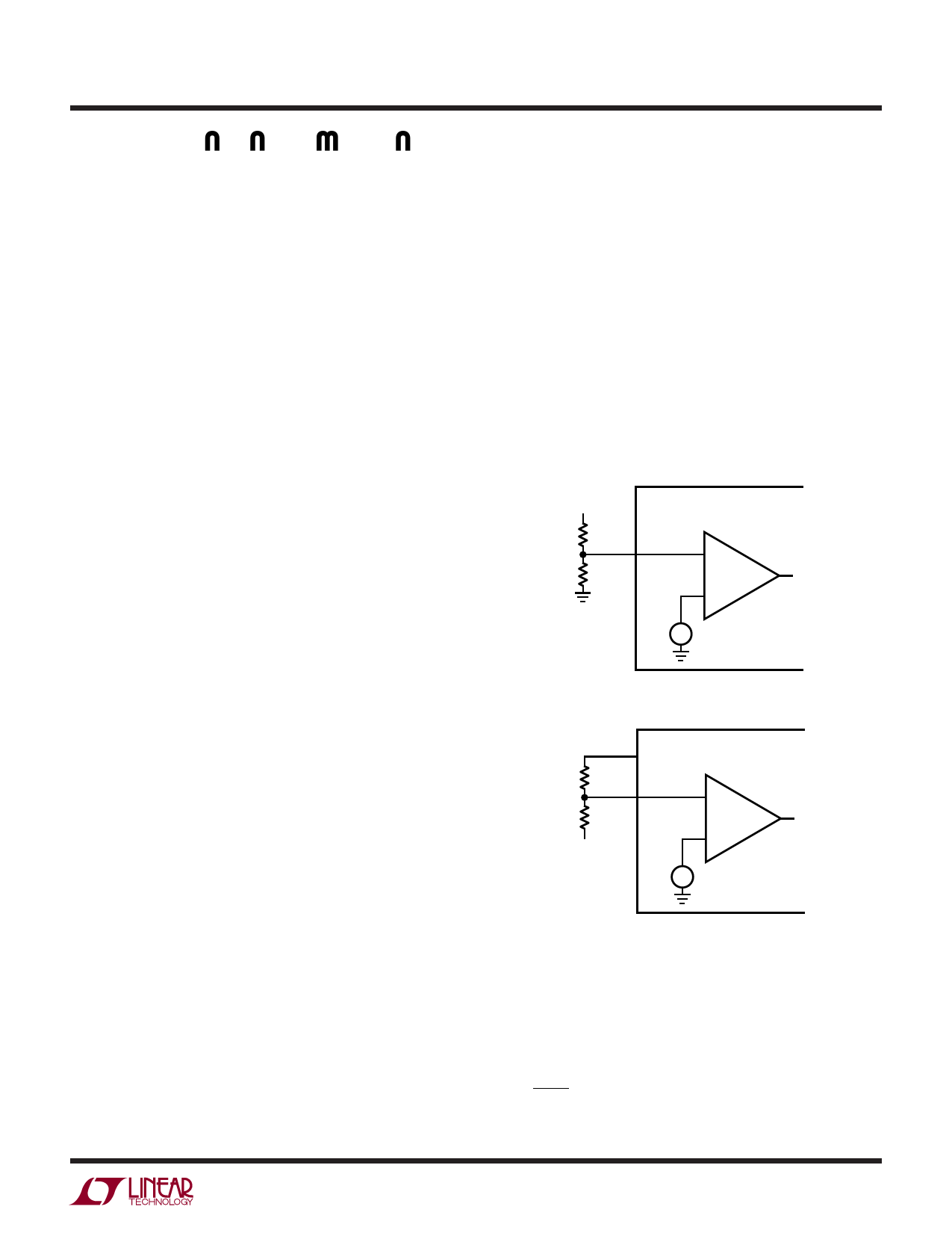
Selecting External Resistors
In a typical positive supply monitoring application, the
ADJx pin connects to a tap point on an external resistive
divider between a positive voltage being monitored and
ground, as shown in Figure 1.
When monitoring a negative supply, the ADJx pin connects
to a tap point on a resistive divider between the negative
voltage being monitored and the buffered reference (REF),
as shown in Figure 2.
VMON
RP2
RP1
ADJx
+
–
0.5V +–
2909 F01
Figure 1. Setting Positive Supply Trip Point
RN1
RN2
VMON
REF
ADJx
+
–
0.5V +–
2909 F02
Figure 2. Setting Negative Supply Trip Point
Normally the user will select a desired trip voltage based
on their supply and acceptable tolerances, and a value of
RN1 or RP1 based on current draw. Current used by the
resistor divider will be approximately:
I = 0.5V
RX1
Recommended range is 1k to 1M.
2909fa
11
Share Link: 