LTC2909 データシートの表示(PDF) - Linear Technology
部品番号
コンポーネント説明
メーカー
LTC2909 Datasheet PDF : 16 Pages
| |||
LTC2909
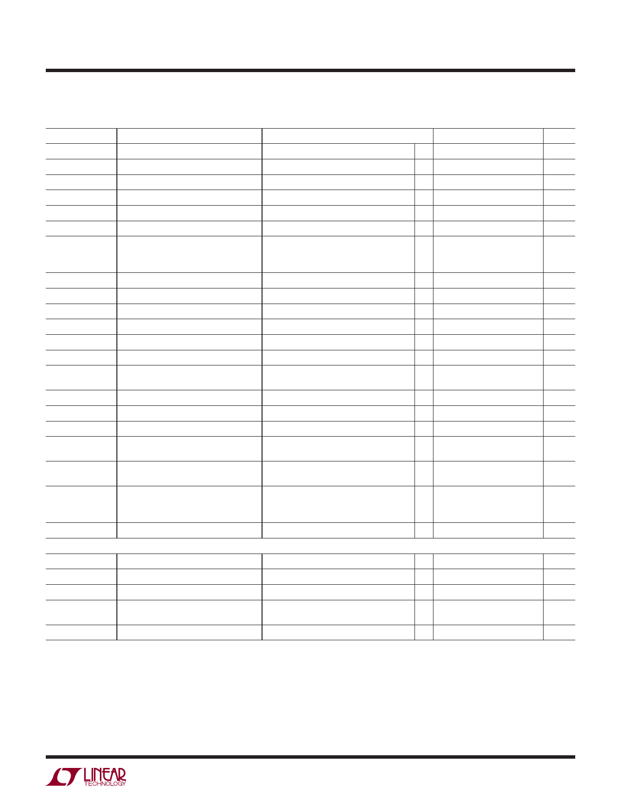
ELECTRICAL CHARACTERISTICS The ● denotes the specifications which apply over the full operating
temperature range, otherwise specifications are at TA = 25°C. VCC = 2.5V (LTC2909-2.5), VCC = 3.3V (LTC2909-3.3), VCC = 5V
(LTC2909-5), ADJ1 = ADJ2 = 0.55V, SEL = floating, unless otherwise noted. (Note 2)
SYMBOL
VCC(MIN)
VCC(SHUNT)
ICC
VRT
ΔVRT
IADJ
VCC(UVLO)
PARAMETER
Operating Supply Voltage
VCC Shunt Regulation Voltage
VCC Input Current
ADJ Input Threshold
ADJ Hysteresis (Note 4)
ADJ Input Current
VCC UVLO Threshold
ΔVCC(UVLO)
VREF
ITMR(UP)
ITMR(DOWN)
t⎯R⎯S⎯T(EXT)
t⎯R⎯S⎯T(INT)
VTMR(DIS)
ΔVTMR(DIS)
VTMR(INT)
ΔVTMR(INT)
tPROP
tUV
VOL(⎯R⎯S⎯T)
UVLO Hysteresis (Note 4)
Buffered Reference Voltage
TMR Pull-Up Current
TMR Pull-Down Current
Reset Timeout Period, External
Reset Timeout Period, Internal
Timer Disable Voltage
Timer Disable Hysteresis
Timer Internal Mode Voltage
Timer Internal Mode Hysteresis
ADJx Comparator Propagation Delay
to ⎯R⎯S⎯T
VCC Undervoltage Detect to ⎯R⎯S⎯T
⎯R⎯S⎯T Output Voltage Low
IOH(⎯R⎯S⎯T)
⎯R⎯S⎯T Output Voltage High Leakage
Three-State Input SEL
VIL
VIH
VZ
ISEL(Z)
Low Level Input Voltage
High Level Input Voltage
Pin Voltage when Left in Open State
Allowable Leakage in Open State
ISEL
SEL Input Current
CONDITIONS
⎯R⎯S⎯T in Correct State
IVCC = 1mA, IVREF = 0
2.175 < VCC < 6V
TMR = VCC
VADJ = 0.55V
LTC2909-2.5
LTC2909-3.3
LTC2909-5
TMR = VCC
VCC > 2.175V, IVREF = ±1mA
VTMR = 1V
VTMR = 1V
CTMR = 2.2nF
VTMR = 0V
VTMR Rising
VTMR Falling
VTMR Falling
VTMR Rising
ADJx Driven Beyond Reset Threshold
(VRTX) by 5mV
VCC Less Than UVLO Threshold
(VCC(UVLO)) by 1%
VCC = 0.5V, I = 5μA
VCC = 1V, I = 100μA
VCC = 3V, I = 2500μA
⎯R⎯S⎯T = VCC
ISEL = 0μA
SEL = VCC or SEL = GND
MIN TYP MAX
● 0.5
● 6.0
6.5
6.9
●
50
150
● 0.4925 0.5000 0.5075
1.5
3.5
10.0
●
±15
● 2.175
● 2.871
● 4.350
2.213
2.921
4.425
2.250
2.970
4.500
0.3
0.7
2.0
● 0.985 1.000 1.015
● –1.5 –2.1 –2.7
● 1.5
2.1
2.7
● 16
20
25
● 150
200
260
● VCC
VCC
VCC
– 0.36 – 0.25 – 0.16
● 60
110
150
● 0.14 0.21 0.27
● 40
70
110
● 50
150
500
UNITS
V
V
μA
V
mV
nA
V
V
V
%
V
μA
μA
ms
ms
V
mV
V
mV
μs
● 50
150
500
μs
●
0.01 0.15
V
●
0.01 0.15
V
●
0.10 0.30
V
●
±1
μA
●
0.4
V
● 1.4
V
0.9
V
● ±5
μA
±10
μA
●
±25
μA
Note 1: Stresses beyond those listed under Absolute Maximum Ratings
may cause permanent damage to the device. Exposure to any Absolute
Maximum Rating condition for extended periods may affect device
reliability and lifetime.
Note 2: All currents into pins are positive; all voltages are referenced to
GND unless otherwise noted.
Note 3: VCC maximum pin voltage is limited by input current. Since the
VCC pin has an internal 6.5V shunt regulator, a low impedance supply
which exceeds 6V may exceed the rated terminal current. Operation
from higher voltage supplies requires a series dropping resistor. See
Applications Information.
Note 4: Threshold voltages have no hysteresis unless the part is in
comparator mode. Hysteresis is one-sided, affecting only invalid-to-valid
transitions. See Applications Information.
2909fb
3
Share Link: 