LTC2919 データシートの表示(PDF) - Linear Technology
部品番号
コンポーネント説明
メーカー
LTC2919 Datasheet PDF : 16 Pages
| |||
LTC2919
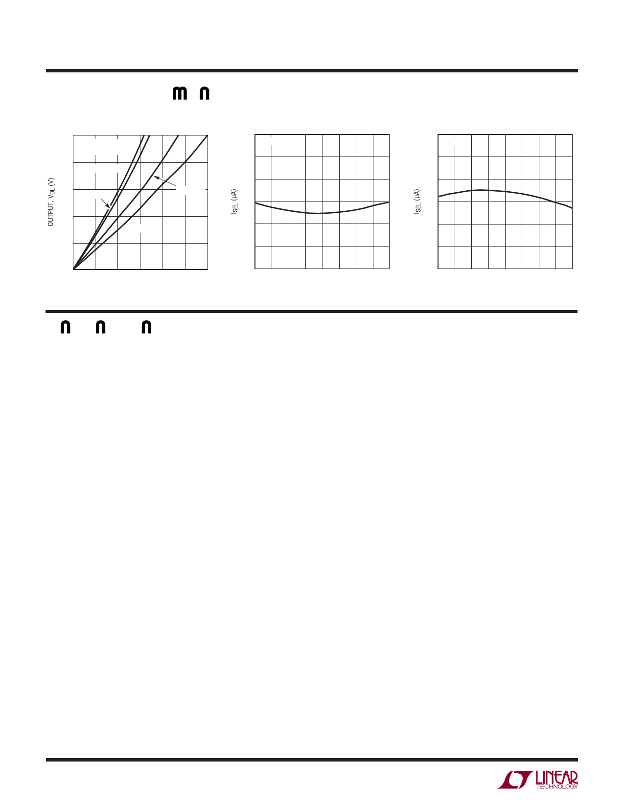
TYPICAL PERFOR A CE CHARACTERISTICS TA = 25°C unless otherwise noted.
OUT1, OUT2, RST VOL vs Output
Sink Current
ISEL vs Temperature
ISEL vs Temperature
1.0
VCC = 3V
NO PULL-UP R
0.8
TA = 150°C
–10
SEL = GND
–12
22
SEL = VCC
20
–14
18
0.6
TA = 125°C
TA = 25°C
–16
16
0.4
TA = –40°C
–18
14
0.2
–20
12
0
0 5 10 15 20 25 30
OUTPUT SINK CURRENT (mA)
2919 G16
–22
–50 –25 0 25 50 75 100 125 150
TEMPERATURE (°C)
2919 G17
10
–50 –25
0 25 50 75 100 125 150
TEMPERATURE (°C)
2919 G18
PI FU CTIO S (MSOP/DFN Package)
SEL (Pin 1): Input Polarity Select Three-State Input. Con-
nect to VCC, GND or leave unconnected in open state to
select one of three possible input polarity combinations
(refer to Table 1).
VCC (Pin 2): Power Supply. Bypass this pin to ground with
a 0.1μF (or greater) capacitor. Operates as a direct supply
input for voltages up to 6V. Operates as a shunt regulator
for supply voltages greater than 6V and should have a
resistor between this pin and the supply to limit VCC input
current to no greater than 10mA. When used without a
current-limiting resistor, pin voltage must not exceed 6V.
UVLO options allow VCC to be used as an accurate third
fixed -10% UV supply monitor.
OUT1 (Pin 3): Open-Drain Logic Output 1. Asserts low
when positive polarity ADJ1 voltage is below threshold or
negative polarity ADJ1 voltage is above threshold. Requires
an external pull-up resistor and may be pulled above VCC.
OUT2 (Pin 4): Open-Drain Logic Output 2. Asserts low
when positive polarity ADJ2 voltage is below threshold
or negative polarity ADJ2 voltage is above threshold.
Requires an external pull-up resistor and may be pulled
above VCC.
RST (Pin 5): Open-Drain Inverted Reset Logic Output.
Asserts low when any positive polarity input voltage is
below threshold or any negative polarity input voltage is
above threshold or VCC is below UVLO threshold. Held
low for a timeout period after all voltage inputs are valid.
6
Requires an external pull-up resistor and may be pulled
above VCC.
GND (Pin 6): Device Ground.
REF (Pin 7): Buffered Reference Output. 1V nominal
reference used for the offset of negative-monitoring ap-
plications. The buffered reference can source and sink
up to 1mA. The reference can drive a capacitive load of
up to 1000pF. Larger capacitance may degrade transient
performance. This pin does not require a bypass capacitor,
nor is one recommended. Leave open if unused.
TMR (Pin 8): Reset Timeout Control. Attach an external
capacitor (CTMR) to GND to set a reset timeout period
of 9ms/nF. A low leakage ceramic capacitor is recom-
mended for timer accuracy. Capacitors larger than 1μF
(9 second timeout) are not recommended. See Applica-
tions Information for further details. Leaving this pin open
generates a minimum timeout of approximately 400μs. A
2.2nF capacitor will generate a 20ms timeout. Tying this
pin to ground will enable the internal 200ms timeout. Ty-
ing this pin to VCC will disable the reset timer and put the
part in comparator mode. Signals from the comparator
outputs will then go directly to RST.
ADJ2 (Pin 9): Adjustable Voltage Input 2. Input to volt-
age monitor comparator 2 (0.5V nominal threshold). The
polarity of the input is selected by the state of the SEL
pin (refer to Table 1). Tie to GND if unused (with SEL =
GND or Open).
2919f
Share Link: 