LTC2919 データシートの表示(PDF) - Linear Technology
部品番号
コンポーネント説明
メーカー
LTC2919 Datasheet PDF : 16 Pages
| |||
LTC2919
APPLICATIO S I FOR ATIO
If the user’s application requires, the SEL pin may be driven
using a three-state buffer which satisfies the VIL, VIH and
leakage conditions of this three-state input pin.
If the state of the SEL pin configures a given input as
“negative polarity,” the voltage at that ADJ pin must be
below the trip point (0.5V nominal), or the corresponding
OUT and RST output will be pulled low. Conversely, if a
given input is configured as “positive polarity”, the ADJ pin
voltage must be above the trip point or the corresponding
OUT and RST will assert low.
Thus, a “negative polarity” input may be used to deter-
mine whether a monitored negative voltage is smaller in
absolute value than it should be (–UV), or a monitored
positive voltage is larger than it should be (+OV). The
opposite is true for a “positive polarity” input (–OV or
+UV). These polarity definitions are also shown in Table
1. For purposes of this data sheet, a negative voltage is
considered “undervoltage” if it is closer to ground than it
should be (e.g., –4.3V for a –5V supply).
Proper configuration of the SEL pin and setting of the
trip-points via external resistors allows for any two fault
conditions to be detected. For example, the LTC2919 may
monitor two supplies (positive, negative or one of each)
for UV or for OV (or one UV and one OV). It may also
monitor a single supply (positive or negative) for both UV
and OV. Tables 2a and 2b show example configurations
for monitoring possible combinations of fault condition
and supply polarity.
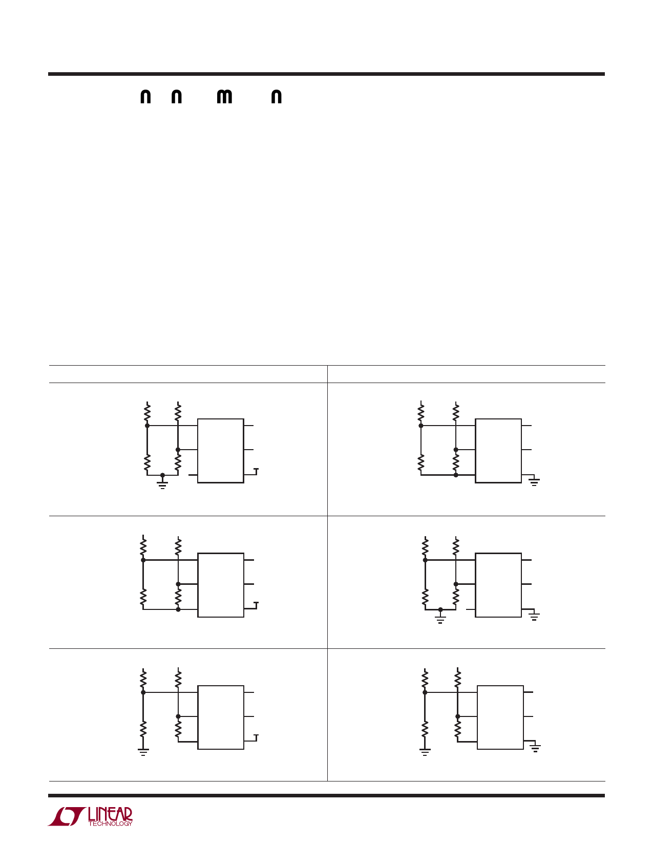
Table 2a. Possible Combinations of Supply Monitoring. For Example Purposes, All Supplies are Monitored at 5% Tolerance and
Connections are Shown Only for ADJ1, ADJ2, REF, SEL, OUT1 and OUT2. Output Pull-up Resistors are Omitted for Clarity.
SEL = VCC
SEL = GND
15V
5V
RP2A
309k
RP2B
115k
ADJ1 OUT1 UV (15V)
–15V
–5V
RN2A
309k
RN2B
137k
ADJ1 OUT1
UV (–15V)
RP1A
11.5k
RP1B
13.7k
ADJ2 OUT2 UV (5V)
REF SEL
RN1A
10.7k
RN1B
13.3k
ADJ2 OUT2 UV (–5V)
REF SEL
2 Positive UV
2 Negative UV
–15V
–5V
RN2A
1.02M
RN2B
137k
ADJ1 OUT1 OV (–15V)
RN1A
30.9k
RN1B
11.8k
ADJ2 OUT2 OV (–5V)
REF SEL
15V
5V
RP2A
619k
RP2B
133k
RP1A
20k
RP1B
13.7k
ADJ1 OUT1 OV (15V)
ADJ2 OUT2 0V (5V)
REF SEL
2 Negative OV
15V
–15V
RP2
309k
RN2
1.02M
ADJ1 OUT1
UV (15V)
RP1
11.5k
RN1
30.9k
ADJ2 OUT2 OV (–15V)
REF SEL
2 Positive OV
15V –15V
RP2
619k
RN2
309k
ADJ1 OUT1
OV (15V)
RP1
RN1
20k 10.7k
ADJ2 OUT2 UV (–15V)
REF SEL
1 Positive UV, 1 Negative OV
1 Positive OV, 1 Negative UV
2919f
9
Share Link: 