LTC2921CGN データシートの表示(PDF) - Linear Technology
部品番号
コンポーネント説明
メーカー
LTC2921CGN Datasheet PDF : 20 Pages
| |||
LTC2921/LTC2922 Series
APPLICATIO S I FOR ATIO
Setting the Supply Monitor Levels
The LTC2921 and LTC2922 series both feature low 0.5V
monitoring thresholds with tight 1% accuracy. To set a
supply monitoring level tightly, design a precision ratio
resistive divider to relate the lowest valid supply voltage to
the maximum specified monitor threshold voltage. Use
resistors with 1% tolerance or better to limit the error due
to mismatch. The basic resistive divider connection for
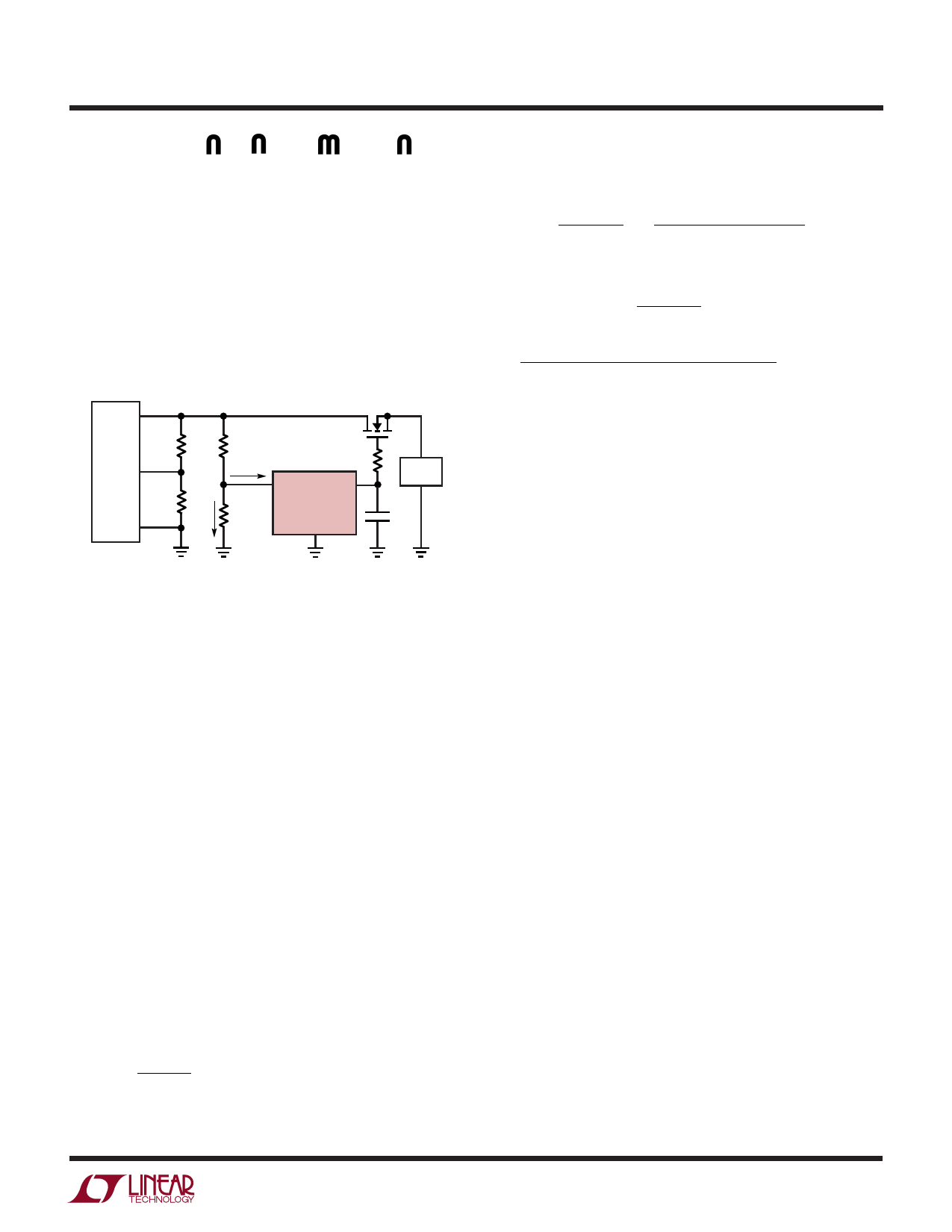
supply monitoring is shown in Figure 5.
VOUT
VFB
GND
VSRC1
+ VQ1 – VL1
Q1
RY1
RB1
RG1
IMON
10Ω
LOAD
VV1 ±0.1µA V1
GATE
RZ1
IA1 RA1
LTC2922
GND
CGATE
DC/DC
CONVERTER
2921/22 F05
Figure 5. Basic Monitor Connection
First, divide the nominal monitor threshold voltage by an
acceptable bias current (IA1), and choose a nearby stan-
dard value for resistor RA1 (see Equation 1).
Next, calculate the bounds on the value of RB1 that
guarantee that the divided minimum supply voltage ex-
ceeds the maximum specified monitor threshold voltage,
and that the minimum specified overvoltage threshold
exceeds the divided maximum supply voltage. Use Equa-
tions 2 and 3 to calculate RB1(MAX) and RB1(MIN) from RA1,
the resistor tolerance (RTOL), the supply voltage, the
monitor threshold and overvoltage specifications, and the
monitor pin leakage current specification.
When the integrated remote sensing switch is closed, the
DC/DC converter will compensate for the IR drop from
drain to source of the external N-channel FET (VQ1(ON)) by
increasing the supply voltage by the same amount. Calcu-
late with VQ1(ON)(MAX) = 0V if the remote sense switch is
not used.
RA1
=
0.500V
IA1
(1)
RB1(MAX) =
RA1
•
1–
1+
RRTTOOLL
•
VSRC1(MIN) – 0.505V
0.505V + 0.1µA •RA1
(2)
RB1(MIN)
=
RA1
•
1+
1–
RRTTOOLL
•
VSRC1(MAX) + VQ1(ON)(MAX) – 0.665V
(3)
0.665V – 0.1µA •RA1
Choose a standard resistor value for RB1 that satisfies the
inequality of Equation 4.
RB1(MIN) ≤ RB1 ≤ RB1(MAX)
(4)
When several standard values meet the requirement,
choose the value closest to RB1(MAX) to set the tightest
monitor threshold. This also allows more headroom for
larger VQ1(ON)(MAX). Alternatively, choose the standard
value closest to RB1(MIN) to set the tightest overvoltage
threshold.
All four monitor input voltages must be between the
monitor threshold and the overvoltage threshold for the
turn-on sequence to begin. Connect unneeded monitor
input pins to any of the utilized monitor input pins.
Selecting the External N-Channel MOSFETs
The GATE pin drives the gate of external N-channel
MOSFETs above VCC to connect the supplies to the loads.
The GATE drive voltage provided by the LTC2921/LTC2922
series is best suited to logic-level and sublogic-level
power MOSFETs. To achieve the lowest switch resistance,
the VCC pin must be connected to the highest supply
voltage.
Consider the application requirements for current, turnoff
speed, on-resistance, gate-source voltage specification,
etc. Refer to the Electrical Specifications and Typical
Performance Curves to determine the GATE voltages for
given VCC voltages over the required range of conditions.
Calculate the minimum gate drive voltage for each moni-
tored supply for use in selecting the FETs. Check the
maximum GATE voltage against the FETs’ gate-source
29212fa
11
Share Link: 