LTC3450EUD データシートの表示(PDF) - Linear Technology
部品番号
コンポーネント説明
メーカー
LTC3450EUD Datasheet PDF : 12 Pages
| |||
LTC3450
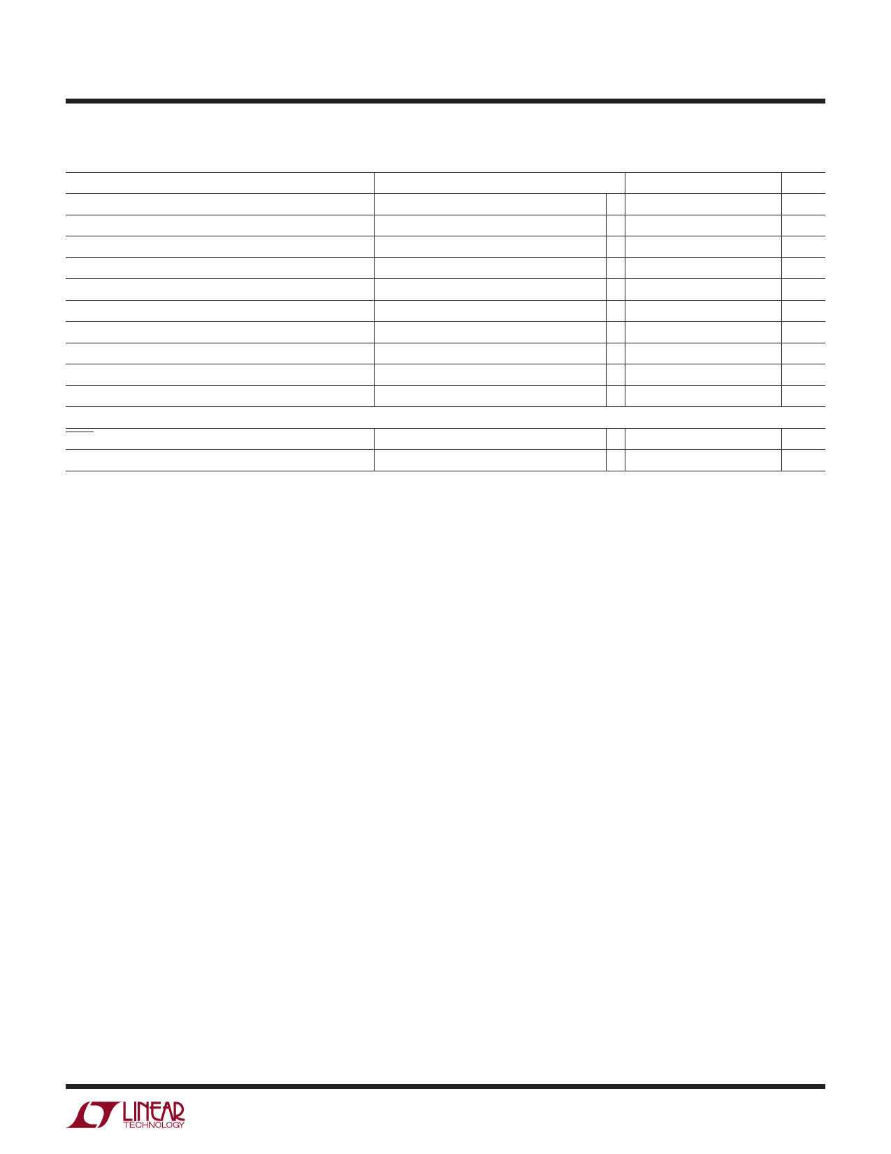
ELECTRICAL CHARACTERISTICS The q denotes the specifications which apply over the full operating
temperature range, otherwise specifications are at TA = 25°C. VIN = 3.6V, VOUT = 5.2V unless otherwise noted.
PARAMETER
V3X Output Voltage
V2X Efficiency
V3X Efficiency
Output Impedance V2X, V3X
VNEG Output Voltage
VNEG Efficiency
Output Impedance VNEG
Switching Frequency Charge Pumps
Switching Frequency Charge Pumps
VNEG to V3X Delay
Logic Inputs
SHDN Pin Threshold
MODE Pin Threshold
CONDITIONS
Load on V3X = 100µA
Load on V2X = 100µA, (Note 2)
Load on V3X = 100µA, (Note 2)
Flying Capacitors = 0.1µF
Load on VNEG = 100µA, VINV = V2X
Load on VNEG = 100µA (Note 2)
Flying Capacitor = 0.1µF
MODE = VIN
MODE = GND
(Note 3)
MIN
q 14.688
q –10.608
3
TYP
15.2
90
80
1
– 10.1
80
1
62.5
3.75
4
MAX
15.912
– 9.792
10
UNITS
V
%
%
kΩ
V
%
kΩ
kHz
kHz
ms
q 0.4
0.77
1.2
V
1.6
V
Note 1: Absolute Maximum Ratings are those values beyond which the life
of a device may be impaired.
Note 2: Specification is guaranteed by design and not 100% tested in
production.
Note 3: Measured from point at which VNEG crosses –5V to point at which
C2– starts switching.
Note 4: The LTC3450E is guaranteed to meet performance specifications
from 0°C to 70°C. Specifications over the – 40°C to 85°C operating
temperature range are assured by design, characterization and correlation
with statistical process controls.
3450f
3
Share Link: 