LTC3780IUH(RevE) データシートの表示(PDF) - Linear Technology
部品番号
コンポーネント説明
メーカー
LTC3780IUH Datasheet PDF : 28 Pages
| |||
LTC3780
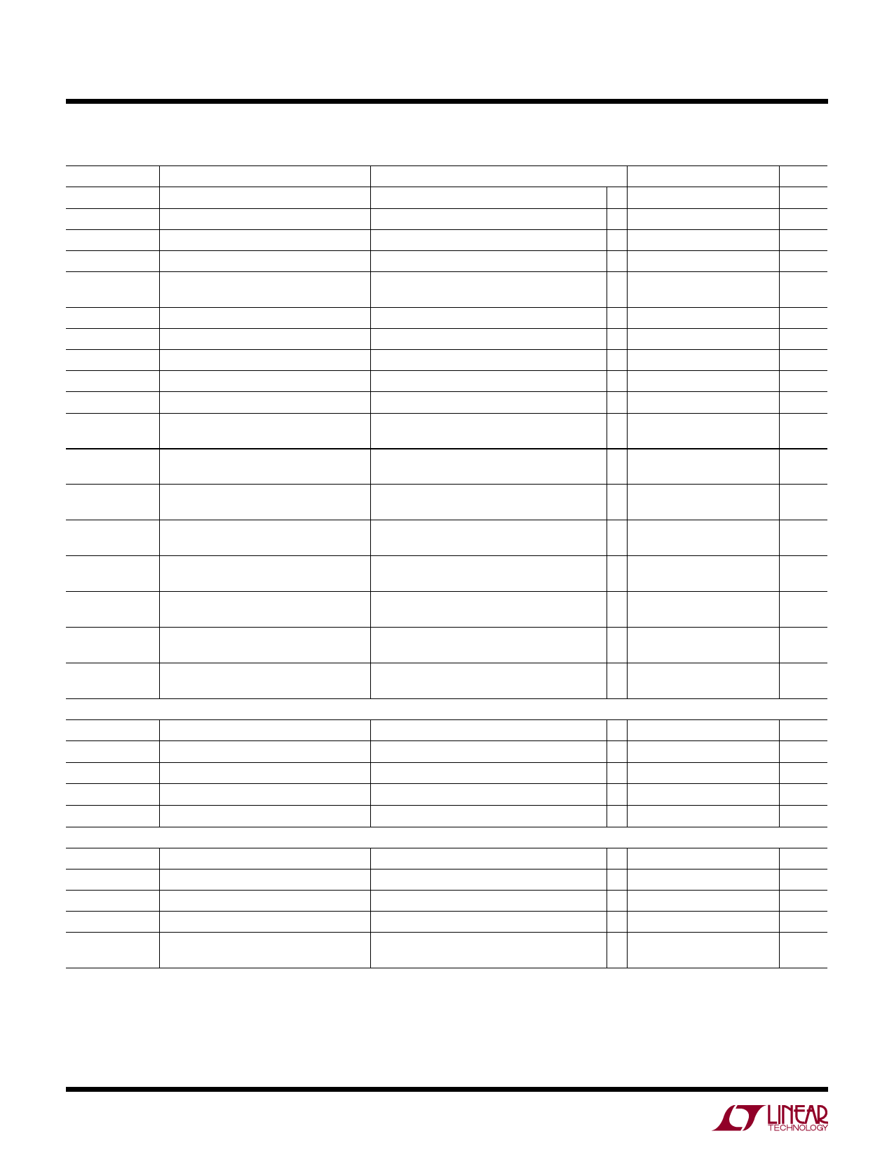
ELECTRICAL CHARACTERISTICS The l denotes the specifications which apply over the full operating
junction temperature range, otherwise specifications are at TA = 25°C. VIN = 15V unless otherwise noted.
SYMBOL
PARAMETER
CONDITIONS
MIN TYP MAX UNITS
DF MAX, Boost Maximum Duty Factor
% Switch C On
99
%
DF MAX, Buck Maximum Duty Factor
% Switch A On (in Dropout)
99
%
VRUN(ON)
ISS
VSENSE(MAX)
RUN Pin On Threshold
Soft-Start Charge Current
Maximum Current Sense Threshold
VSENSE(MIN,BUCK)
TG1, TG2 tr
TG1, TG2 tf
BG1, BG2 tr
BG1, BG2 tf
TG1/BG1 t1D
Minimum Current Sense Threshold
TG Rise Time
TG Fall Time
BG Rise Time
BG Fall Time
TG1 Off to BG1 On Delay,
Switch C On Delay
VRUN Rising
VRUN = 2V
Boost: VOSENSE = VREF – 50mV
Buck: VOSENSE = VREF – 50mV
Discontinuous Mode
CLOAD = 3300pF (Note 5)
CLOAD = 3300pF (Note 5)
CLOAD = 3300pF (Note 5)
CLOAD = 3300pF (Note 5)
CLOAD = 3300pF Each Driver
1
1.5
2
V
0.5
1.2
μA
l
160 185
mV
l –95 –110 –150
mV
–6
mV
50
ns
45
ns
45
ns
55
ns
80
ns
BG1/TG1 t2D
BG1 Off to TG1 On Delay,
Synchronous Switch D On Delay
CLOAD = 3300pF Each Driver
80
ns
TG2/BG2 t3D
TG2 Off to BG2 On Delay,
Synchronous Switch B On Delay
CLOAD = 3300pF Each Driver
80
ns
BG2/TG2 t4D
BG2 Off to TG2 On Delay,
Switch A On Delay
CLOAD = 3300pF Each Driver
80
ns
Mode
Transition 1
BG1 Off to BG2 On Delay,
Switch A On Delay
CLOAD = 3300pF Each Driver
250
ns
Mode
Transition 2
BG2 Off to BG1 On Delay,
Synchronous Switch D On Delay
CLOAD = 3300pF Each Driver
250
ns
tON(MIN,BOOST)
Minimum On-Time for Main Switch in Switch C (Note 6)
Boost Operation
200
ns
tON(MIN,BUCK)
Minimum On-Time for Synchronous
Switch in Buck Operation
Switch B (Note 6)
180
ns
Internal VCC Regulator
VINTVCC
Internal VCC Voltage
∆VLDO(LOADREG) Internal VCC Load Regulation
VEXTVCC
EXTVCC Switchover Voltage
∆VEXTVCC(HYS) EXTVCC Switchover Hysteresis
∆VEXTVCC
EXTVCC Switch Drop Voltage
Oscillator and Phase-Locked Loop
7V < VIN < 30V, VEXTVCC = 5V
ICC = 0mA to 20mA, VEXTVCC = 5V
ICC = 20mA, VEXTVCC Rising
ICC = 20mA, VEXTVCC = 6V
l 5.7
6
6.3
V
0.2
2
%
l 5.4
5.7
V
300
mV
150 300
mV
fNOM
fLOW
fHIGH
RPLLIN
IPLLLPF
Nominal Frequency
Lowest Frequency
Highest Frequency
PLLIN Input Resistance
Phase Detector Output Current
VPLLFLTR = 1.2V
VPLLFLTR = 0V
VPLLFLTR = 2.4V
fPLLIN < fOSC
fPLLIN > fOSC (Note 9)
260 300 330
kHz
170 200 220
kHz
340 400 440
kHz
50
kΩ
–15
μA
15
μA
3780fe
4
Share Link: 