LTC4218CGN(RevB) データシートの表示(PDF) - Linear Technology
部品番号
コンポーネント説明
メーカー
LTC4218CGN Datasheet PDF : 16 Pages
| |||
LTC4218
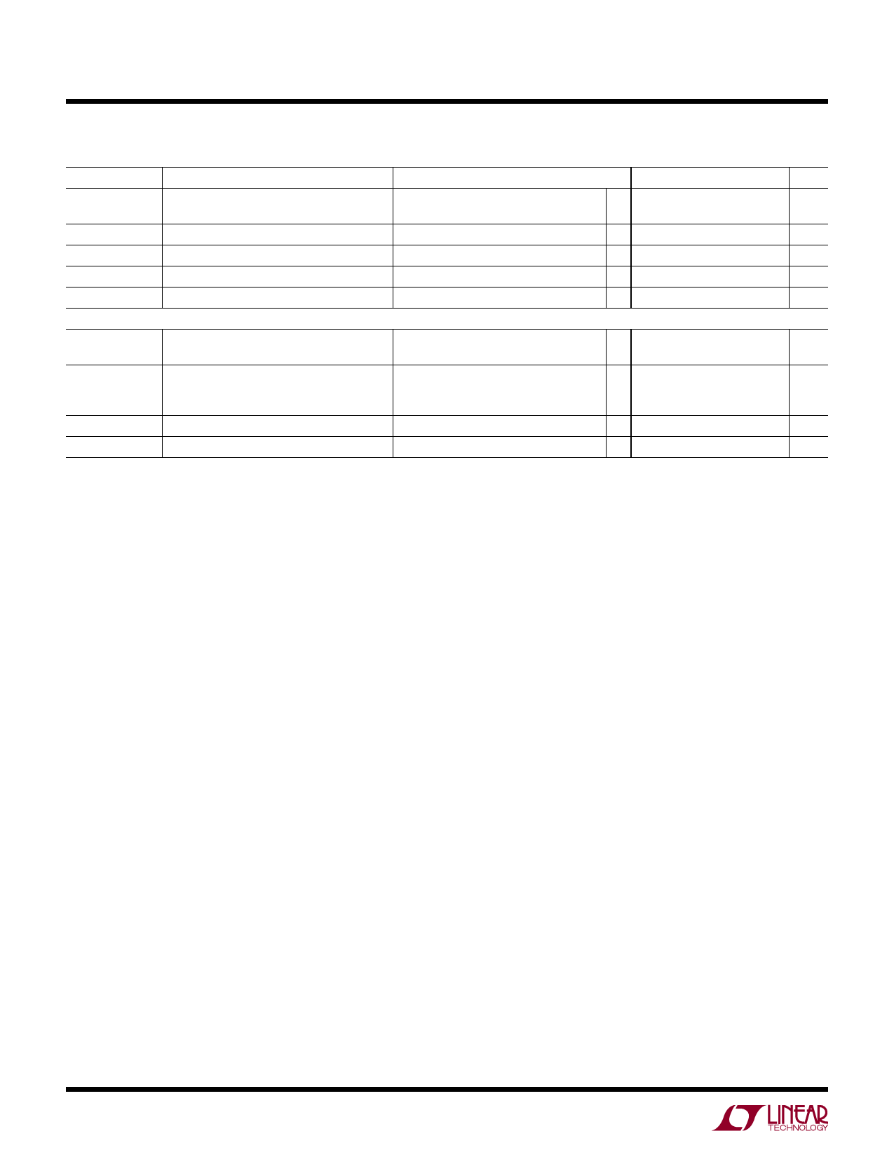
ELECTRICAL CHARACTERISTICS The ● denotes the specifications which apply over the full operating
temperature range, otherwise specifications are at TA = 25°C. VDD = 12V unless otherwise noted.
SYMBOL
PARAMETER
CONDITIONS
MIN TYP MAX UNITS
ITIMER(RATIO)
TIMER Pin Current Ratio ITIMER(DN)/
ITIMER(UP)
IMON(FS)
IMON Fullscale Output Current
IMON(OFF)
IMON Pin Offset Current
GIMON
IMON Pin Gain
AC Characteristics
VSENSE+ – VSENSE– = 15mV
VSENSE+ – VSENSE– = 1mV
VSENSE+ – VSENSE– = 15mV and 1mV
● 1.6
2
2.7
%
● 94
100
106
μA
●
±0
±6
μA
● 6.47 6.67 6.87 μA/mV
tPHL(GATE)
tPHL(SENSE)
Input High (OV), Input Low (UV) to GATE VGATE < 16.5V Falling
●
Low Propagation Delay
VSENSE+ – VSENSE– High to GATE Low
Propagation Delay
VFB = 0, Step (VSENSE+ – VSENSE–) to
●
60mV, CGATE = 1.5nF, VGATE < 16.5V
Falling
3
5
μs
0.2
1
μs
tD(ON)
Turn-On Delay
Step VUV to 2V, VGATE > 13V
● 50
100
150
ms
Note 1: Stresses beyond those listed under Absolute Maximum Ratings
may cause permanent damage to the device. Exposure to any Absolute
Maximum Rating condition for extended periods may affect device
reliability and lifetime.
Note 2: All currents into pins are positive, all voltages are referenced to
GND unless otherwise specified.
Note 3: An internal clamp limits the GATE pin to a maximum of 6.5V above
the SOURCE pin. Driving either GATE or SOURCE pin to voltages beyond
the clamp may damage the device.
4218fb
4
Share Link: 