LTC6801HG-TRPBF(RevC) データシートの表示(PDF) - Linear Technology
部品番号
コンポーネント説明
メーカー
LTC6801HG-TRPBF Datasheet PDF : 28 Pages
| |||
LTC6801
ELECTRICAL CHARACTERISTICS The l denotes the specifications which apply over the full operating
temperature range, otherwise specifications are at TA = 25°C, V+ = 43.2V, V– = 0V unless otherwise noted.
SYMBOL
PARAMETER
CONDITIONS
MIN TYP MAX
LTC6801 Single Ended Digital I/O Specifications (SLT, SLTOK Pins)
VIH
Digital Input Voltage High
VIL
Digital Input Voltage Low
SLT Pin
SLT Pin
l
2
l
0.5
VODL
Digital Output Voltage Low, Open Drain
SLT Pin, 10k to VREG
VOH
Digital Output Voltage High
SLTOK Pin, 10k to V–
VOL
Digital Output Voltage Low
SLTOK Pin, 10k to VREG
IPU-ST
Pull-Up Current
SLT Pin
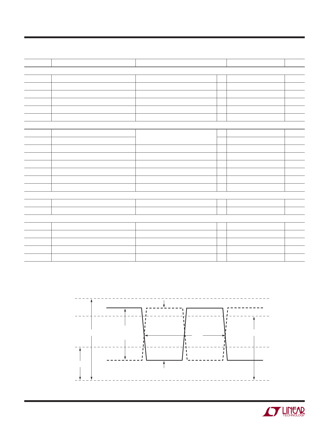
LTC6801 Differential Digital Input Specifications (SIN/SIN, EIN/EIN Pins) (See Figure 1)
l
0.3
l VREG – 0.3
l
0.3
l 2.5
5
10
VIDH
VIDL
VIL
VIH
VDHYS
VOPEN
Minimum Differential Input Voltage High Differential Voltage Applied Between SIN l 1.7
Minimum Differential Input Voltage Low
and SIN or EIN and EIN
l
Valid Input Voltage Low
Low Side of Differential Signal, Ref. to V– l
0
Valid Input Voltage High
High Side of Differential Signal, Ref. to V– l 2.5
Differential Input Hysteresis
Open Circuit Voltage
l
2
–1.7
1.2
6
1
2.5
3
RINCM
Input Resistance, Common Mode
l 100
150
RINDIFF
Input Resistance, Differential
Between SIN to SIN, EIN to EIN
l 200
300
LTC6801 Differential Digital Output Specifications (SOUT/SOUT, EOUT/EOUT Pins)
VODH
Digital Output Voltage High
Output Pins Loaded With 100k to V–
l VREG – 0.4
VODL
Digital Output Voltage Low
Output Pins Loaded With 100k to VREG
l
0.4
LTC6801 Three-Level Digital Input Specifications (OV0, OV1, UV0, UV1, HYST, DC, CC0 and CC1 Pins)
V3IH
Three-Level Digital Input Voltage High
l VREG – 0.3
V3IM
Three-Level Digital Input Voltage Mid
l VREF – 0.3
VREF + 0.3
V3IL
Three-Level Digital Input Voltage Low
IPU
Pull-Up Current
Pins DC, CC0, CC1, UV0 and UV1
IPD
Pull-Down Current
Pins HYST, OV0 and OV1
l
0.3
l 0.5
1
2
l 0.5
1
2
UNITS
V
V
V
V
V
µA
V
V
V
V
V
V
kΩ
kΩ
V
V
V
V
V
µA
µA
Note 1: Stresses beyond those listed under Absolute Maximum Ratings
may cause permanent damage to the device. Exposure to any Absolute
Maximum Rating condition for extended periods may affect device
reliability and lifetime.
Note 2: VCELL refers to the voltage applied across the following pin
combinations: Cn to Cn – 1 for n = 2 to 12, C1 to V–.
Note 3: Guaranteed by continuous monitoring supply current
specifications, not subject to test.
EIN
MAX, VIH
VIDH
(VALID HIGH WHEN
EIN – EIN ≥ VIDH)
TENA
MIN, VIH
EIN
MAX, VIL
V– = 0V
VIDL
(VALID LOW WHEN EIN – EIN ≤ VIDL)
Figure 1. Differential Input Specifications
4
For more information www.linear.com/LTC6801
6801 F01
6801fc
Share Link: 