LTC6801HG-PBF データシートの表示(PDF) - Linear Technology
部品番号
コンポーネント説明
メーカー
LTC6801HG-PBF Datasheet PDF : 28 Pages
| |||
LTC6801
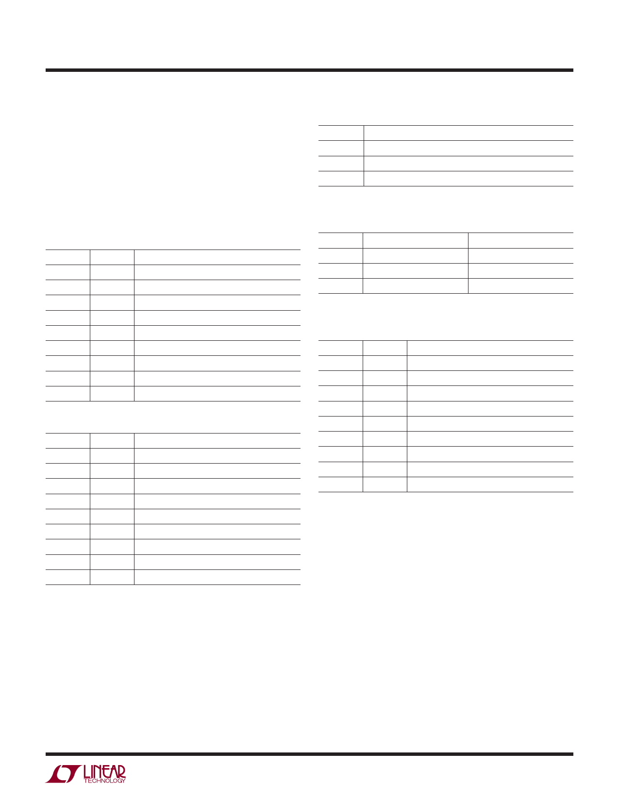
PIN FUNCTIONS
UV0, UV1 (Pin 33, Pin 34): Undervoltage Three-Level
Inputs. These pins may be tied to VREG, VREF or V–. UV1
and UV0 select the undervoltage threshold and each pin
has an internal pull-up to VREG. See Table 2.
OV0, OV1 (Pin 35, Pin 36): Overvoltage Three-Level
Inputs. These pins may be tied to VREG, VREF or V–. OV1
and OV0 select the overvoltage threshold and each pin
has an internal pull-down to V–. See Table 1.
Table 1. Overvoltage Inputs
OV1
OV0
OVERVOLTAGE THRESHOLD (V)
VREG
VREG
VREG
VREF
VREF
VREF
V–
V–
V–
VREG
VREF
V–
VREG
VREF
V–
VREG
VREF
V–
4.498
4.403
4.307
4.211
4.116
4.020
3.924
3.828
3.733
Table 2. Undervoltage Inputs
UV1
UV0
UNDERVOLTAGE THRESHOLD (V)
VREG
VREG
VREG
VREF
VREF
VREF
V–
V–
V–
VREG
VREF
V–
VREG
VREF
V–
VREG
VREF
V–
2.871
2.680
2.489
2.297
2.106
1.914
1.723
1.531
0.766
Table 3. Duty Cycle Select
DC
NOMINAL CYCLE TIME*
VREG
15.5ms
VREF
Approximately 130ms
V–
Approximately 500ms
*Cycle time based on LTC6801 measuring 12 cells and 2 temperatures.
Table 4. Hysteresis Select
HYST
UV HYSTERESIS*
OV HYSTERESIS
VREG
500mV
200mV
VREF
250mV
V–
0mV
100mV
0mV
*UV hysteresis is disabled when the undervoltage threshold is set to 0.766V.
Table 5. Cell Count Select
CC1
CC0
VREG
VREG
VREG
VREF
VREF
VREF
V–
V–
V–
VREG
VREF
V–
VREG
VREF
V–
VREG
VREF
V–
CELL COUNT
12
11
10
9
8
7
6
5
4
6801fb
9
Share Link: 