LTC6991HS6 データシートの表示(PDF) - Linear Technology
部品番号
コンポーネント説明
メーカー
LTC6991HS6 Datasheet PDF : 24 Pages
| |||
LTC6991
Pin Functions (DCB/S6)
GND (Pin 5/Pin 2): Ground. Tie to a low inductance ground
plane for best performance.
OUT (Pin 6/Pin 6): Oscillator Output. The OUT pin swings
from GND to V+ with an output resistance of approximately
30Ω. When driving an LED or other low impedance load a
series output resistor should be used to limit source/sink
current to 20mA.
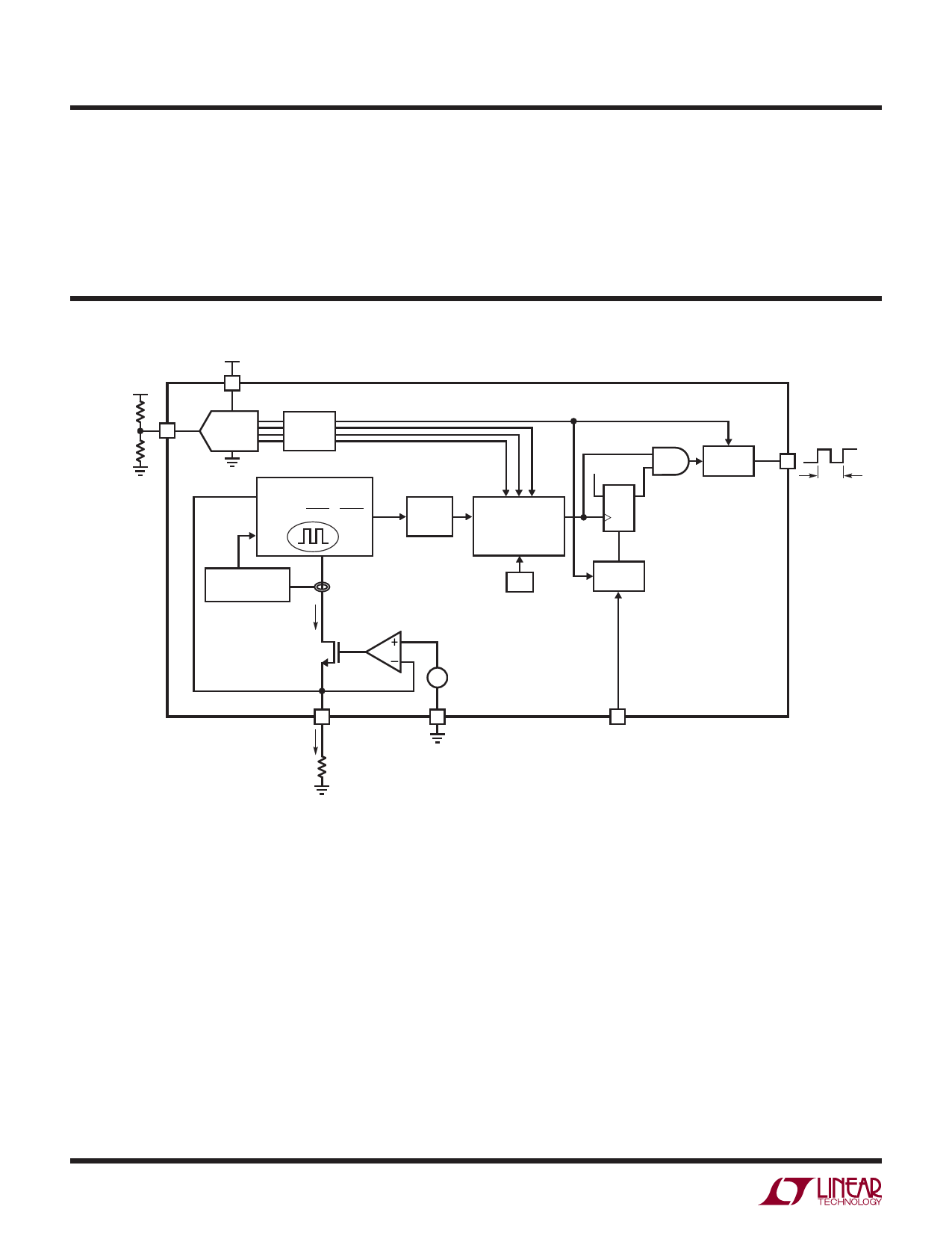
Block Diagram (S6 package pin numbers shown)
R1
4 DIV
R2
5
V+
4-BIT A/D
CONVERTER
DIGITAL
FILTER
MASTER OSCILLATOR
tMASTER
=
1µs
50kΩ
=
VSET
ISET
MCLK FIXED
DIVIDER
÷ 1024
HALT OSCILLATOR
IF ISET < 500nA
ISET
POL BIT
PROGRAMMABLE
DIVIDER
÷1, 8, 64, 512
4096, 215, 218, 221
POR
V+
DQ
R
INPUT
POLARITY
VSET = 1V
SET
3
ISET
RSET
+– 1V
GND
2
RST
1
OUTPUT
POLARITY
OUT
6
tOUT
6991 BD
6991f
Share Link: 