LX2203 データシートの表示(PDF) - Microsemi Corporation
部品番号
コンポーネント説明
メーカー
LX2203 Datasheet PDF : 11 Pages
| |||
LX2203
TM
®
Li-Ion Battery Charger
PRODUCTION DATA SHEET
ABSOLUTE MAXIMUM RATINGS
Supply Voltage (VIN)....................................................................................... -0.3V to 7V
Input Signals (SHDN, EN,CMP) ...................................................................... -0.3V to 7V
Battery Charging Current (IBAT)....................................................................................1.2A
Operating Junction Temperature................................................................... -40C to 150°C
Storage Temperature Range.........................................................................-65°C to 150°C
RoHS / Pb-free Peak Package Solder Reflow Temp(40 seconds max. exposure) ............260°C (+0 -5)
Note: Exceeding these ratings could cause damage to the device. All voltages are with respect to
Ground. Currents are positive into, negative out of specified terminal.
THERMAL DATA
LD Plastic Micro Leadframe Package 10-Pin
THERMAL RESISTANCE-JUNCTION TO AMBIENT, θJA
49°C/W
Junction Temperature Calculation: TJ = TA + (PD x θJA).
The θJA numbers are guidelines for the thermal performance of the device/pc-board system. All of the
above assume no ambient airflow.
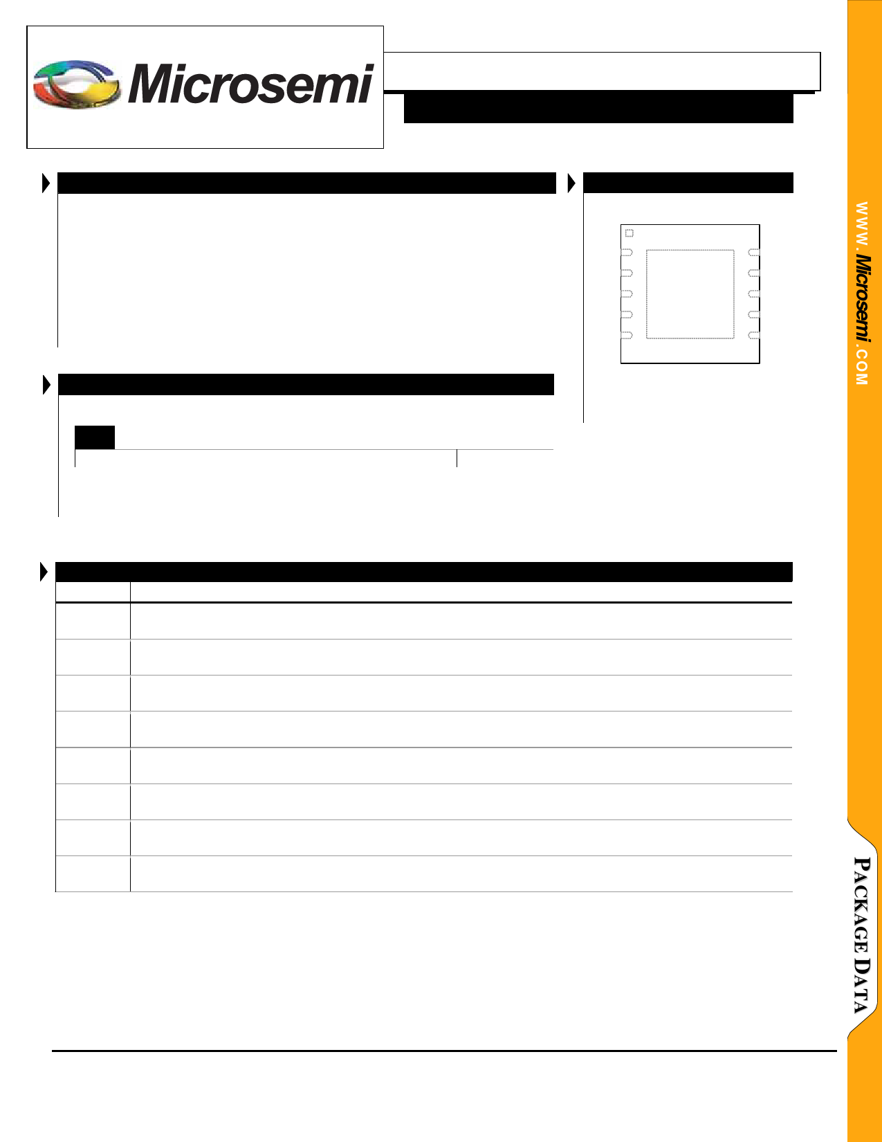
PACKAGE PIN OUT
VIN 1
10 BAT
VIN 2
9 BAT
STAT 3
8 CMP
CTP 4 Connect Bottom to 7 EN
Power GND
GND 5
6 CCP
LD PACKAGE
(Top View)
RoHS / Pb-free 100% Matte Tin Lead Finish
Name
BAT
CCP
CMP
CTP
EN
GND
STAT
VIN
FUNCTIONAL PIN DESCRIPTION
Description
Charging Output - This pin is wired to the positive terminal of the battery. (The negative battery terminal is wired
to GND.)
Charge Current Programming Pin - A resistor (Rccp) is connected between this pin and GND. See application
section for programming information.
Compensation Pin – Apply a 0.01µF capacitor between CMP and VIN pins.
Charge Termination Programming Pin – A resistor (Rctp) is connected between this pin and GND See
application section for programming information.
Enable - Applying a TTL compatible Hi signal enables the charger, a Low signal disables the charger and puts it
in sleep mode.
Common Ground.
Status - This pin is a logic low level when the battery is being charged. Pin can sink up to 5mA.
Voltage Input – Supply Voltage. Must be greater than VBAT to charge.
Copyright © 2004
Rev. 1.0a, 2005-08-10
Microsemi
Integrated Products Division
11861 Western Avenue, Garden Grove, CA. 92841, 714-898-8121, Fax: 714-893-2570
Page 2
Share Link: 