M24C16-BN3TG/W гғҮгғјгӮҝгӮ·гғјгғҲгҒ®иЎЁзӨәпјҲPDFпјү - STMicroelectronics
йғЁе“Ғз•ӘеҸ·
гӮігғігғқгғјгғҚгғігғҲиӘ¬жҳҺ
гғЎгғјгӮ«гғј
M24C16-BN3TG/W Datasheet PDF : 29 Pages
| |||
M24C16, M24C08, M24C04, M24C02, M24C01
Table 8. AC Measurement Conditions
Symbol
Parameter
CL
Load Capacitance
Input Rise and Fall Times
Input Levels
Input and Output Timing Reference Levels
Min.
Max.
100
50
0.2VCC to 0.8VCC
0.3VCC to 0.7VCC
Unit
pF
ns
V
V
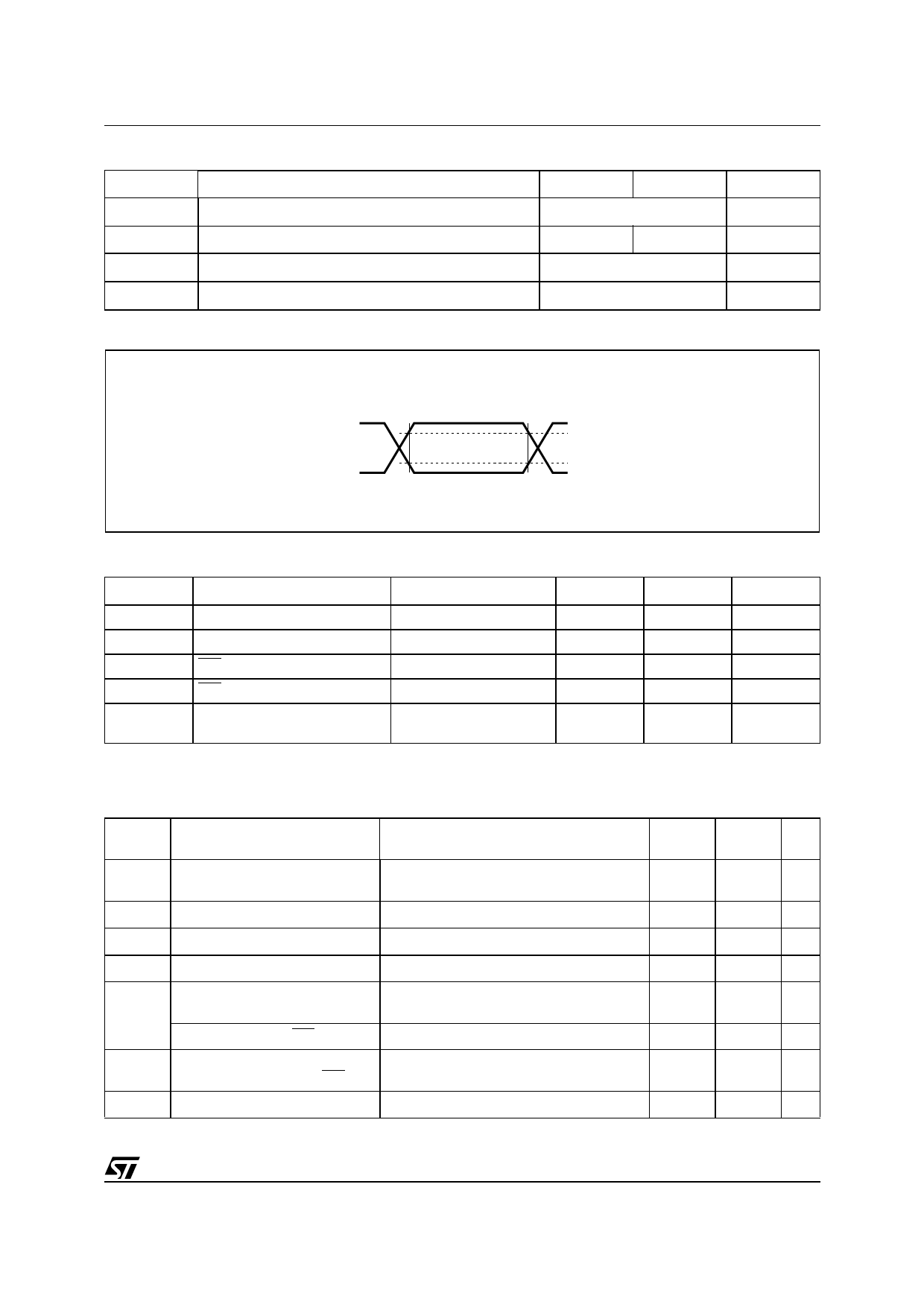
Figure 10. AC Measurement I/O Waveform
Input Levels
0.8VCC
0.2VCC
Input and Output
Timing Reference Levels
0.7VCC
0.3VCC
AI00825B
Table 9. Input Parameters
Symbol
Parameter1,2
CIN
Input Capacitance (SDA)
CIN
Input Capacitance (other pins)
ZWCL
WC Input Impedance
ZWCH
WC Input Impedance
tNS
Pulse width ignored
(Input Filter on SCL and SDA)
Note: 1. TA = 25В°C, f = 400kHz
2. Sampled only, not 100% tested.
Test Condition
VIN < 0.5 V
VIN > 0.7VCC
Single glitch
Min.
Max.
Unit
8
pF
6
pF
5
70
kв„Ұ
500
kв„Ұ
100
ns
Table 10. DC Characteristics (M24Cxx, Device Grade 6)
Symbol
Parameter
Test Condition
(in addition to those in Table 5.)
ILI
Input Leakage Current
(SCL, SDA)
VIN = VSS or VCC
ILO Output Leakage Current
VOUT = VSS or VCC, SDA in Hi-Z
ICC Supply Current
VCC=5V, fc=400kHz (rise/fall time < 30ns)
ICC1 Stand-by Supply Current
Input Low Voltage
VIL
(E2, E1, E0, SCL, SDA)
Input Low Voltage (WC)
VIN = VSS or VCC , VCC = 5 V
VIH
Input High Voltage
(E2, E1, E0, SCL, SDA, WC)
VOL Output Low Voltage
IOL = 3 mA, VCC = 5 V
Note: 1. This range is Not for New Design, and will soon be replaced by the M24Cxx-Wxx6 range.
Min.
вҖ“0.45
вҖ“0.45
0.7VCC
Max. Unit
Вұ 2 ВөA
Вұ 2 ВөA
2
mA
1
ВөA
0.3VCC V
0.5
V
VCC+1 V
0.4
V
15/29
Share Link: 