M24C16-BN3TG/W гғҮгғјгӮҝгӮ·гғјгғҲгҒ®иЎЁзӨәпјҲPDFпјү - STMicroelectronics
йғЁе“Ғз•ӘеҸ·
гӮігғігғқгғјгғҚгғігғҲиӘ¬жҳҺ
гғЎгғјгӮ«гғј
M24C16-BN3TG/W Datasheet PDF : 29 Pages
| |||
M24C16, M24C08, M24C04, M24C02, M24C01
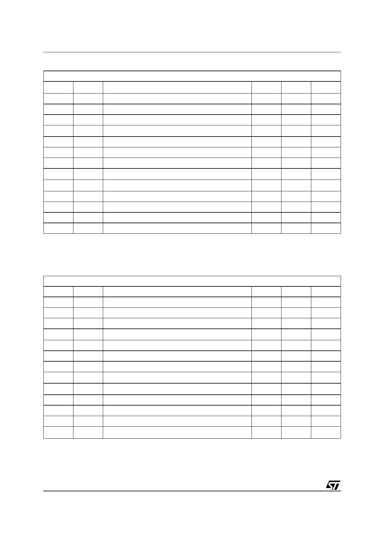
Table 15. AC Characteristics (M24Cxx, Device Grade 6)
Test conditions specified in Table 8. and Table 5.
Symbol
Alt.
Parameter
Min.4
Max.4
Unit
fC
fSCL Clock Frequency
400
kHz
tCHCL
tHIGH Clock Pulse Width High
600
ns
tCLCH
tLOW Clock Pulse Width Low
1300
ns
tDL1DL2 2
tF
SDA Fall Time
20
300
ns
tDXCX
tSU:DAT Data In Set Up Time
100
ns
tCLDX
tHD:DAT Data In Hold Time
0
ns
tCLQX
tDH
Data Out Hold Time
200
ns
tCLQV 3
tAA
Clock Low to Next Data Valid (Access Time)
200
900
ns
tCHDX 1
tSU:STA Start Condition Set Up Time
600
ns
tDLCL
tHD:STA Start Condition Hold Time
600
ns
tCHDH
tSU:STO Stop Condition Set Up Time
600
ns
tDHDL
tBUF Time between Stop Condition and Next Start Condition
1300
ns
tW
tWR
Write Time
5
ms
Note: 1. For a reSTART condition, or following a Write cycle.
2. Sampled only, not 100% tested.
3. To avoid spurious START and STOP conditions, a minimum delay is placed between SCL=1 and the falling or rising edge of SDA.
4. This is preliminary data for M24Cxx-Wxx3.
Table 16. AC Characteristics (M24Cxx, Device Grade 3; M24Cxx-W, Device Grade 6 or 3)
Test conditions specified in Table 8. and Table 5. or Table 6.
Symbol
Alt.
Parameter
Min.
Max.
Unit
fC
fSCL Clock Frequency
400
kHz
tCHCL
tHIGH Clock Pulse Width High
600
ns
tCLCH
tLOW Clock Pulse Width Low
1300
ns
tDL1DL2 2
tF
SDA Fall Time
20
300
ns
tDXCX
tSU:DAT Data In Set Up Time
100
ns
tCLDX
tHD:DAT Data In Hold Time
0
ns
tCLQX
tDH
Data Out Hold Time
200
ns
tCLQV 3
tAA
Clock Low to Next Data Valid (Access Time)
200
900
ns
tCHDX 1
tSU:STA Start Condition Set Up Time
600
ns
tDLCL
tHD:STA Start Condition Hold Time
600
ns
tCHDH
tSU:STO Stop Condition Set Up Time
600
ns
tDHDL
tBUF Time between Stop Condition and Next Start Condition
1300
ns
tW
tWR
Write Time
10 or4 5
ms
Note: 1. For a reSTART condition, or following a Write cycle.
2. Sampled only, not 100% tested.
3. To avoid spurious START and STOP conditions, a minimum delay is placed between SCL=1 and the falling or rising edge of SDA.
4. 10ms write time is offered on the standard device. 5ms write time is offered on new products bearing the Process Identification letter
вҖңWвҖқ or вҖңGвҖқ on the package, as described in Table 24..
18/29
Share Link: 