EVAL-AD7466CB データシートの表示(PDF) - Analog Devices
部品番号
コンポーネント説明
メーカー
EVAL-AD7466CB Datasheet PDF : 28 Pages
| |||
AD7466/AD7467/AD7468
TIMING SPECIFICATIONS
For all devices, VDD = 1.6 V to 3.6 V; TA = TMIN to TMAX, unless otherwise noted. Sample tested at 25°C to ensure compliance. All input
signals are specified with tr = tf = 5 ns (10% to 90% of VDD) and timed from a voltage level of 1.4 V.
Table 4.
Parameter
fSCLK
tCONVERT
Acquisition Time
Limit at TMIN, TMAX
3.4
10
20
150
16 × tSCLK
12 × tSCLK
10 × tSCLK
Unit
MHz max
kHz min
kHz min
kHz min
780
640
tQUIET
10
t1
10
t2
55
t3
55
ns max
ns max
ns min
ns min
ns min
ns max
t4
140
ns max
t5
0.4 tSCLK
ns min
t6
0.4 tSCLK
ns min
t7
10
ns min
t8
60
ns max
7
ns min
Description
Mark/space ratio for the SCLK input is 40/60 to 60/40.
1.6 V ≤ VDD ≤ 3 V; minimum fSCLK at which specifications are guaranteed.
VDD = 3.3 V; minimum fSCLK at which specifications are guaranteed.
VDD = 3.6 V; minimum fSCLK at which specifications are guaranteed.
AD7466.
AD7467.
AD7468.
Acquisition time/power-up time from power-down. See the Terminology section.
The acquisition time is the time required for the part to acquire a full-scale step
input value within ±1 LSB or a 30 kHz ac input value within ±0.5 LSB.
VDD = 1.6 V.
1.8 V ≤ VDD ≤ 3.6 V.
Minimum quiet time required between bus relinquish and the start of the next
conversion.
Minimum CS pulse width.
CS to SCLK setup time. If VDD = 1.6 V and fSCLK = 3.4 MHz, t2 has to be 192 ns
minimum in order to meet the maximum figure for the acquisition time.
Delay from CS until SDATA is three-state disabled. Measured with the load circuit
in Figure 2 and defined as the time required for the output to cross the VIH or VIL
voltage.
Data access time after SCLK falling edge. Measured with the load circuit in Figure 2
and defined as the time required for the output to cross the VIH or VIL voltage.
SCLK low pulse width.
SCLK high pulse width.
SCLK to data valid hold time. Measured with the load circuit in Figure 2 and
defined as the time required for the output to cross the VIH or VIL voltage.
SCLK falling edge to SDATA three-state. t8 is derived from the measured time taken
by the data outputs to change 0.5 V when loaded with the circuit in Figure 2. The
measured number is then extrapolated back to remove the effects of charging or
discharging the 50 pF capacitor. This means that the time, t8, quoted in the timing
characteristics, is the true bus relinquish time of the part, and is independent of
the bus loading.
SCLK falling edge to SDATA three-state.
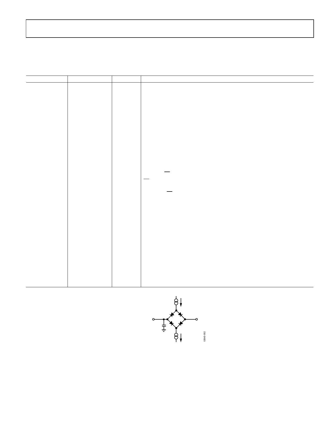
200μA
IOL
TO OUTPUT
PIN CL
50pF
1.4V
200μA
IOH
Figure 2. Load Circuit for Digital Output Timing Specifications
Rev. C | Page 9 of 28
Share Link: 