M25PE40 データシートの表示(PDF) - STMicroelectronics
部品番号
コンポーネント説明
メーカー
M25PE40 Datasheet PDF : 37 Pages
| |||
M25PE40
SUMMARY DESCRIPTION
The M25PE40 is a 4Mbit (512K x 8 bit) Serial
Paged Flash Memory accessed by a high speed
SPI-compatible bus.
The memory can be written or programmed 1 to
256 Bytes at a time, using the Page Write or Page
Program instruction. The Page Write instruction
consists of an integrated Page Erase cycle fol-
lowed by a Page Program cycle.
The memory is organized as 8 sectors, each con-
taining 256 pages. Each page is 256 Bytes wide.
Thus, the whole memory can be viewed as con-
sisting of 2048 pages, or 524,288 Bytes.
The memory can be erased a page at a time, using
the Page Erase instruction, or a sector at a time,
using the Sector Erase instruction.
The top sector of the memories can be Write Pro-
tected by Hardware (TSL).
Table 1. Signal Names
C
Serial Clock
D
Serial Data Input
Q
Serial Data Output
S
Chip Select
TSL
Top Sector Lock
Reset
Reset
VCC
Supply Voltage
VSS
Ground
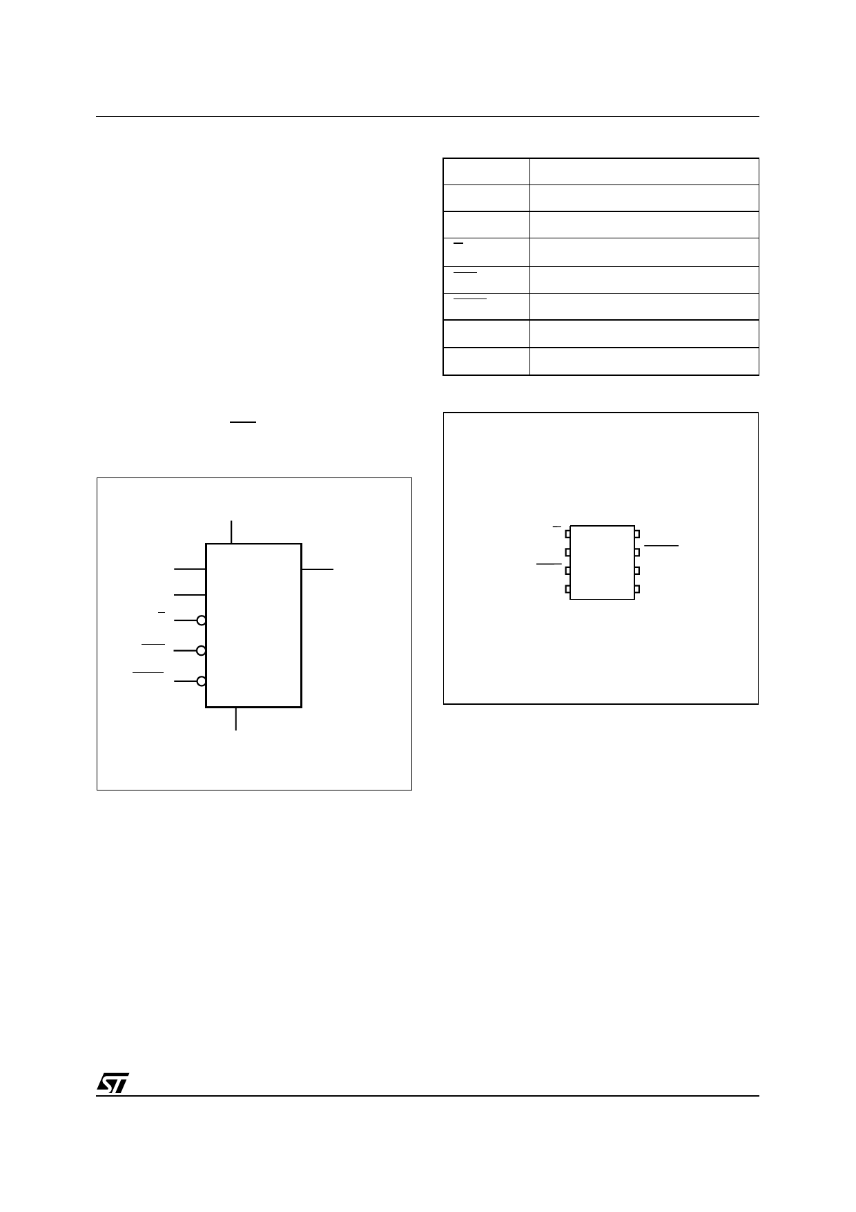
Figure 3. VDFPN and SO Connections
Figure 2. Logic Diagram
VCC
D
C
S
TSL
Reset
Q
M25PE40
M25PE40
S1
Q2
TSL 3
VSS 4
8 VCC
7 Reset
6C
5D
AI09703C
VSS
AI09704C
Note: 1. There is an exposed die paddle on the underside of the
MLP8 package. This is pulled, internally, to VSS, and
must not be allowed to be connected to any other voltage
or signal line on the PCB.
2. See PACKAGE MECHANICAL section for package di-
mensions, and how to identify pin-1.
5/37
Share Link: 