M29W512B データシートの表示(PDF) - STMicroelectronics
部品番号
コンポーネント説明
メーカー
M29W512B Datasheet PDF : 18 Pages
| |||
M29W512B
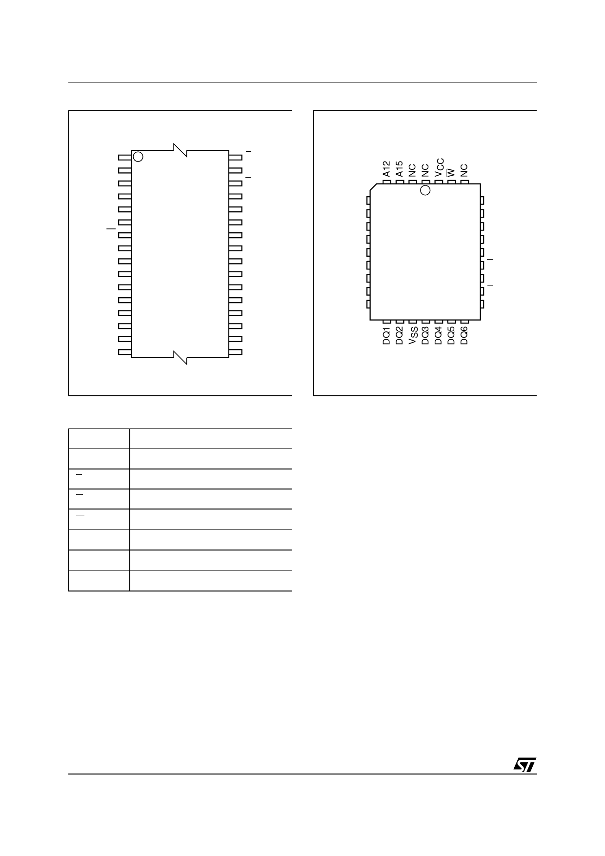
Figure 2. TSOP Connections
A11
A9
A8
A13
A14
NC
W
VCC
NC
NC
A15
A12
A7
A6
A5
A4
1
32
8 M29W512B 25
9
24
16
17
AI02976
G
A10
E
DQ7
DQ6
DQ5
DQ4
DQ3
VSS
DQ2
DQ1
DQ0
A0
A1
A2
A3
Figure 3. PLCC Connections
A7
A6
A5
A4
A3 9
A2
A1
A0
DQ0
1 32
M29W512B
17
A14
A13
A8
A9
25 A11
G
A10
E
DQ7
AI02755
Table 1. Signal Names
A0-A15
Address Inputs
DQ0-DQ7 Data Inputs/Outputs
E
Chip Enable
G
Output Enable
W
Write Enable
VCC
Supply Voltage
VSS
Ground
NC
Not Connected Internally
SUMMARY DESCRIPTION
The M29W512B is a 512 Kbit (64Kb x8) non-vola-
tile memory that can be read, erased and repro-
grammed. These operations can be performed
using a single low voltage (2.7 to 3.6V) supply. On
power-up the memory defaults to its Read mode
where it can be read in the same way as a ROM or
EPROM.
Program and Erase commands are written to the
Command Interface of the memory. An on-chip
Program/Erase Controller simplifies the process of
programming or erasing the memory by taking
care of all of the special operations that are re-
quired to update the memory contents. The end of
a program or erase operation can be detected and
any error conditions identified. The command set
required to control the memory is consistent with
JEDEC standards.
Chip Enable, Output Enable and Write Enable sig-
nals control the bus operation of the memory.
They allow simple connection to most micropro-
cessors, often without additional logic.
The memory is offered in TSOP32 (8 x 14mm) and
PLCC32 packages and it is supplied with all the
bits erased (set to ’1’).
2/18
Share Link: 