M28010 データシートの表示(PDF) - STMicroelectronics
部品番号
コンポーネント説明
メーカー
M28010 Datasheet PDF : 23 Pages
| |||
M28010
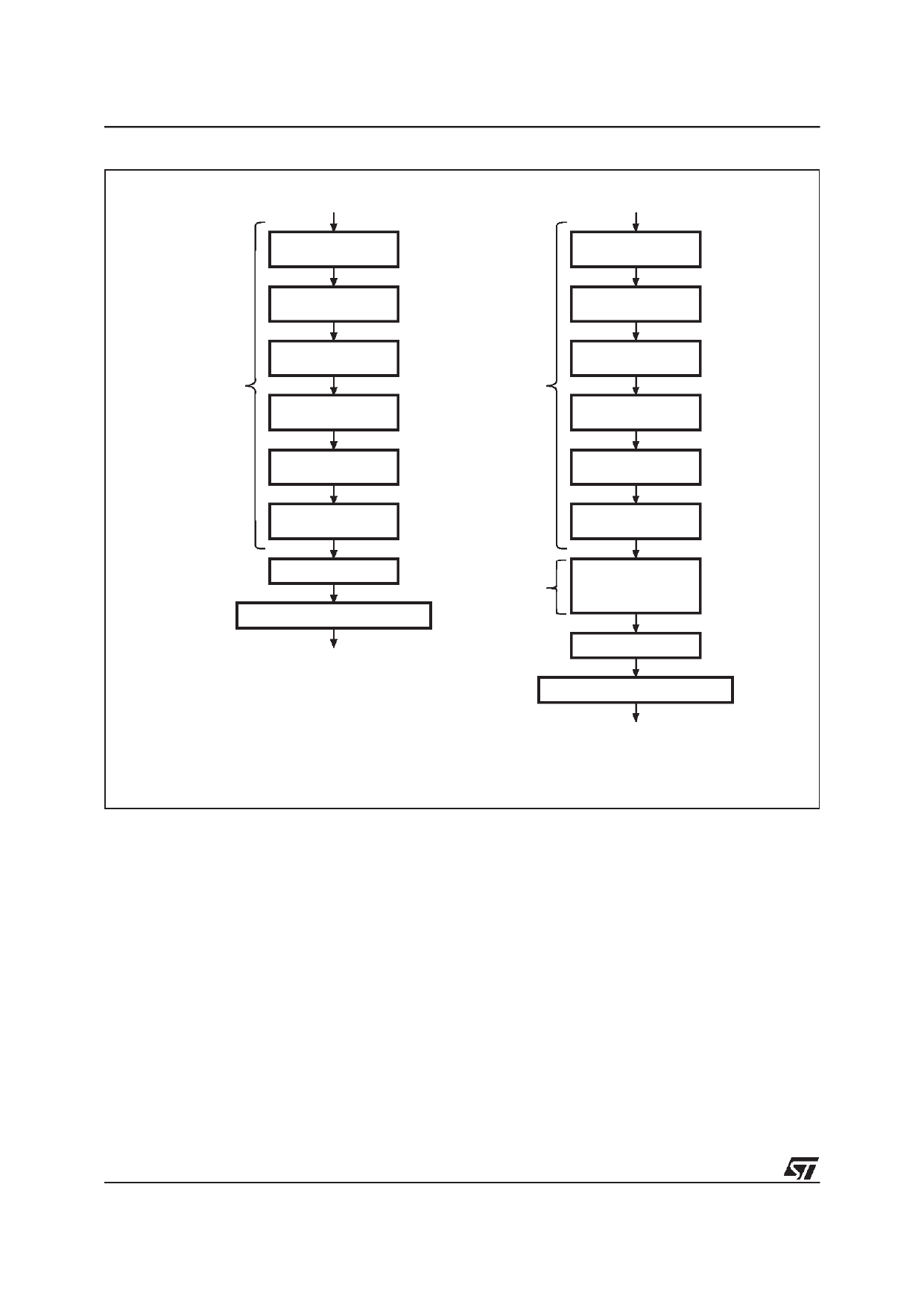
Figure 5. Software Data Protection Disable Algorithms (with or without Memory Write)
SDP is Enabled and
Application needs to Disable it
SDP is Enabled and
Application needs to Write Data
Write AAh in
Address 5555h
Write AAh in
Address 5555h
Write 55h in
Address 2AAAh
Write 55h in
Address 2AAAh
Page Write
Timing
Write 80h in
Address 5555h
Write AAh in
Address 5555h
Page Write
Timing
Write 80h in
Address 5555h
Write AAh in
Address 5555h
Write 55h in
Address 2AAAh
Write 55h in
Address 2AAAh
Write 20h in
Address 5555h
Write 20h in
Address 5555h
Time Out (tWLQ5H)
Wait for write completion (tQ5HQ5X)
SDP is Disabled
Physical
Write
Instructions
Write data
in any addresses
within one page
Time Out (tWLQ5H)
Wait for write completion (tQ5HQ5X)
DATA has been written
and SDP is Disabled
AI02226B
can be detected by reading the status of the Data
Polling and the Toggle Bit functions on DQ7 and
DQ6.
Page Write
The Page Write mode allows up to 128 bytes to be
written on a single page in a single go. This is
achieved through a series of successive Write
operations, no two of which are separated by more
than the tWLQ5H value (as specified in Table 9A to
Table 9C).
The page write can be initiated during any byte
write operation. Following the first Byte Write
instruction, the host may send another address
and data with a minimum data transfer rate of:
1/tWLQ5H.
The internal write cycle can start at any instant
after tWLQ5H. Once initiated, the write operation is
internally timed, and continues, uninterrupted,
until completion.
All bytes must be located on the same page
address (A16-A7 must be the same for all bytes).
Otherwise, the Page Write operation is not
executed. The Page Write Abort event is indicated
to the application via DQ1 (as described on page
8).
As with the single byte Write operation, described
above, the DQ5, DQ6 and DQ7 lines can be used
to detect the beginning and end of the internally
controlled phase of the Page Write cycle.
Software Data Protection (SDP)
The device offers a software-controlled write-
protection mechanism that allows the user to
inhibit all write operations to the device, including
chip erase. This can be useful for protecting the
6/23
Share Link: 