MSK5041 データシートの表示(PDF) - M.S. Kennedy
部品番号
コンポーネント説明
メーカー
MSK5041 Datasheet PDF : 6 Pages
| |||
APPLICATION NOTES CONT'D
RF HIGH:
It is very important that the DC voltage returned to the RF high pin from the output be as noise and oscillation free as possible.
This voltage helps to determine the final output and therefore must be a clean voltage. Excessive noise or oscillation can cause the
device to have an incorrect output voltage. Proper PC board layout techniques can help to achieve a noise free voltage at the RF
high pin.
MODES OF OPERATION:
Under heavy loads, the MSK 5041 operates in full PWM mode. Each pulse from the oscillator sets the internal PWM latch that
turns on the high-side MOSFET. As the high-side switch turns off, the synchronous rectifier latch is set. 60ns later the low-side
MOSFET turns on until the start of the next clock cycle or until the inductor current crosses zero. Under fault conditions the current
exceeds the ±100mV current-limit threshold and the high-side switch turns off.
At light loads the inductor current does not exceed the 30mV threshold set by the minimum-current comparator. When this
occurs, the MSK 5041 goes into idle mode, skipping most of the oscillator pulses in order to reduce the switching frequency and
cut back gate-charge losses. The oscillator is gated off at light loads because the minimum-current comparator immediately resets
the high-side latch at the start of each cycle. Refer to Table 1 for the operational characteristics.
OPERATIONAL CHARACTERISTICS
ENABLE
LOAD
DESCRIPTION
0
X
DEVICE DISABLED
1
LOW <10%
PULSE SKIPPING MODE DISCONTINUOUS INDUCTOR CURRENT
1
MED <30%
PULSE SKIPPING MODE CONTINUOUS INDUCTOR CURRENT
1
HIGH >30%
CONSTANT FREQ. PWM MODE CONTINUOUS INDUCTOR CURRENT
TABLE 1
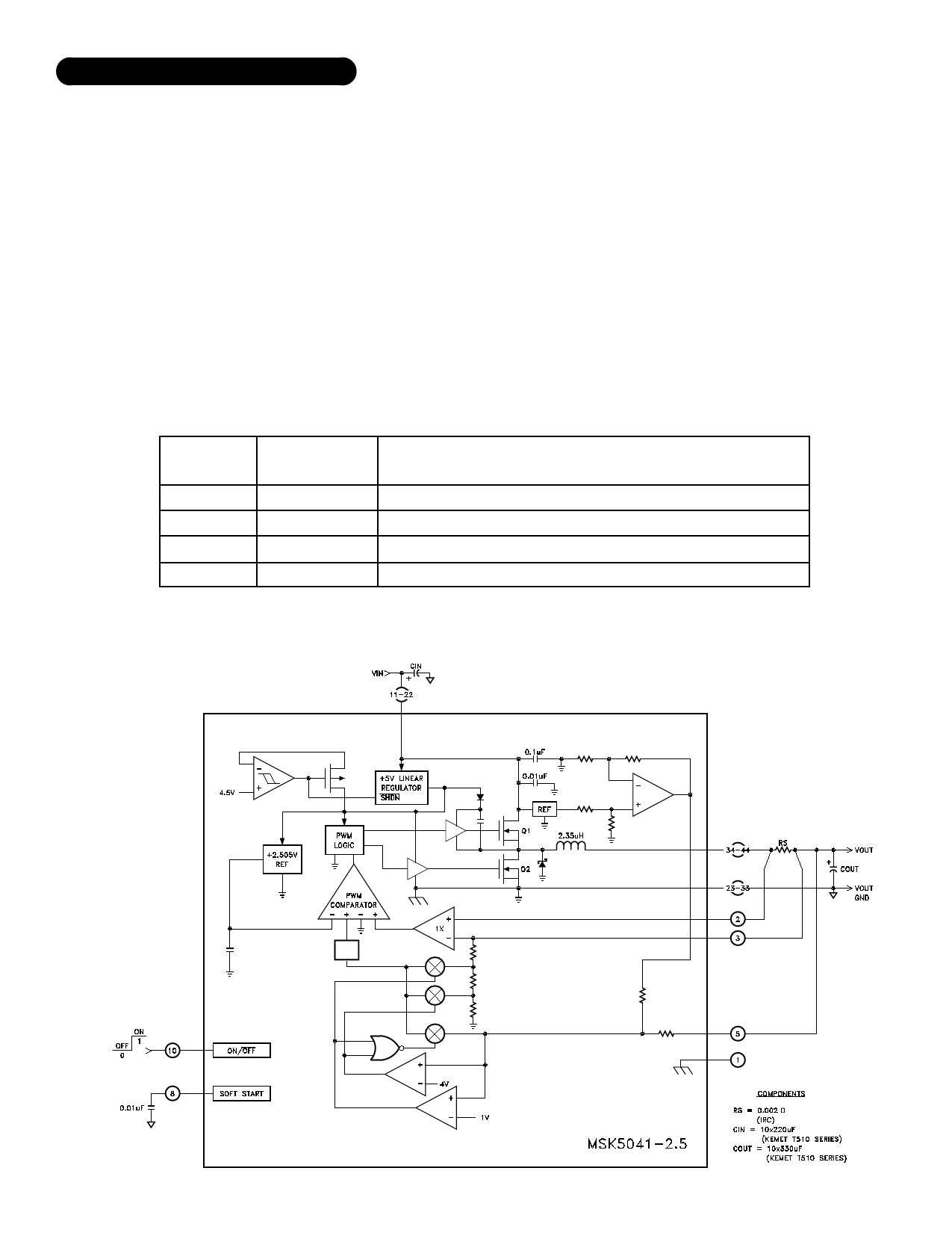
TYPICAL 2.5V APPLICATION CIRCUIT
4
PRELIMINARY Rev. - 6/01
Share Link: 