CY7C4211-10JCT データシートの表示(PDF) - Cypress Semiconductor
部品番号
コンポーネント説明
メーカー
CY7C4211-10JCT Datasheet PDF : 18 Pages
| |||
CY7C4421/4201/4211/4221
CY7C4231/4241/4251
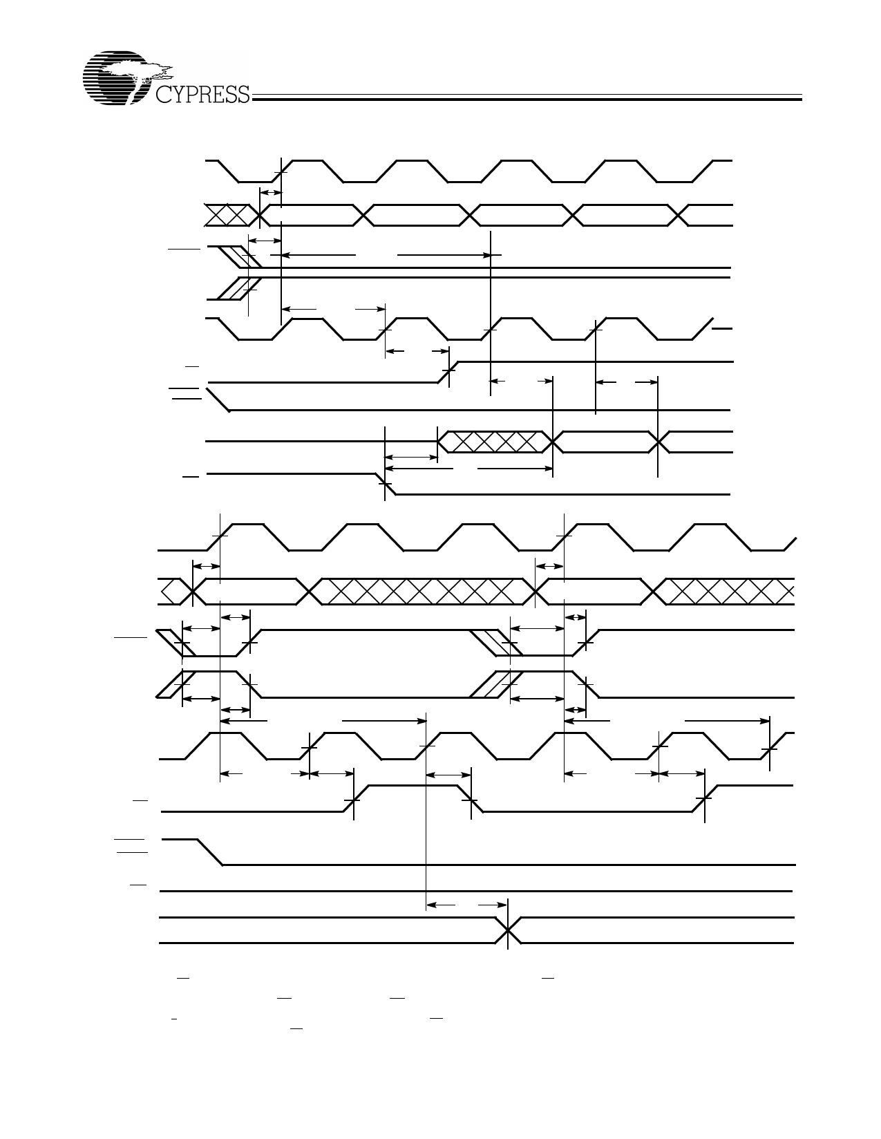
Switching Waveforms (continued)
First Data Word Latency after Reset with Simultaneous Read and Write
WCLK
tDS
D0–D8
D0 (FIRSTVALID Write)
D1
D2
tENS
WEN1
WEN2
(if applicable)
[20]
tFRL
RCLK
tSKEW1
EF
REN1,
REN2
tREF
tA[21]
D3
D4
tA
Q0 –Q8
OE
tOLZ
tOE
D0
D1
Empty Flag Timing
WCLK
D0 –D8
WEN1
tDS
DATAWRITE1
tENS
tENH
tDS
DATAWRITE2
tENS
tENH
WEN2
(if applicable)
RCLK
tENS
EF
tENH tFRL [20]
tSKEW1
tREF
tENS
tENH tFRL [20]
tREF
tSKEW1
tREF
REN1,
REN2
OE
LOW
Q0 –Q8
tA
DATA IN OUTPUT REGISTER
DATA Read
Notes:
17. The clocks (RCLK, WCLK) can be free-running during reset.
18. Holding WEN2/LD HIGH during reset will make the pin act as a second enable pin. Holding WEN2/LD LOW during reset will make the pin act as a load enable
for the programmable flag offset registers.
19. After reset, the outputs will be LOW if OE = 0 and three-state if OE=1.
20. When tSKEW1 > minimum specification, tFRL (maximum) = tCLK + tSKEW1. When tSKEW1 < minimum specification, tFRL (maximum) = either 2*tCLK + tSKEW1 or
tCLK + tSKEW1. The Latency Timing applies only at the Empty Boundary (EF = LOW).
21. The first word is available the cycle after EF goes HIGH, always.
Document #: 38-06016 Rev. *B
Page 10 of 18
Share Link: 