M29DW323DB90N6 データシートの表示(PDF) - STMicroelectronics
部品番号
コンポーネント説明
メーカー
M29DW323DB90N6
STMicroelectronics

M29DW323DB90N6 Datasheet PDF : 49 Pages
| |||
M29DW323DT, M29DW323DB
SUMMARY DESCRIPTION
The M29DW323D is a 32 Mbit (4Mb x8 or 2Mb
x16) non-volatile memory that can be read, erased
and reprogrammed. These operations can be per-
formed using a single low voltage (2.7 to 3.6V)
supply. On power-up the memory defaults to its
Read mode where it can be read in the same way
as a ROM or EPROM.
The device features an asymmetrical block archi-
tecture. The M29DW323D has an array of 8 pa-
rameter and 63 main blocks and is divided into two
Banks, A and B, providing Dual Bank operations.
While programming or erasing in Bank A, read op-
erations are possible in Bank B and vice versa.
Only one bank at a time is allowed to be in pro-
gram or erase mode. The bank architecture is
summarized in Table 2. M29DW323DT locates the
Parameter Blocks at the top of the memory ad-
dress space while the M29DW323DB locates the
Parameter Blocks starting from the bottom.
M29DW323D has an extra 32 KWord (x16 mode)
or 64 KByte (x8 mode) block, the Extended Block,
that can be accessed using a dedicated com-
mand. The Extended Block can be protected and
so is useful for storing security information. How-
ever the protection is irreversible, once protected
the protection cannot be undone.
Each block can be erased independently so it is
possible to preserve valid data while old data is
erased. The blocks can be protected to prevent
accidental Program or Erase commands from
modifying the memory. Program and Erase com-
mands are written to the Command Interface of
the memory. An on-chip Program/Erase Controller
simplifies the process of programming or erasing
the memory by taking care of all of the special op-
erations that are required to update the memory
contents. The end of a program or erase operation
can be detected and any error conditions identi-
fied. The command set required to control the
memory is consistent with JEDEC standards.
Chip Enable, Output Enable and Write Enable sig-
nals control the bus operation of the memory.
They allow simple connection to most micropro-
cessors, often without additional logic.
The memory is offered in TSOP48 (12x20mm),
TFBGA63 (7x11mm, 0.8mm pitch) and TFBGA48
(6x8mm, 0.8mm pitch) packages. The memory is
supplied with all the bits erased (set to ’1’).
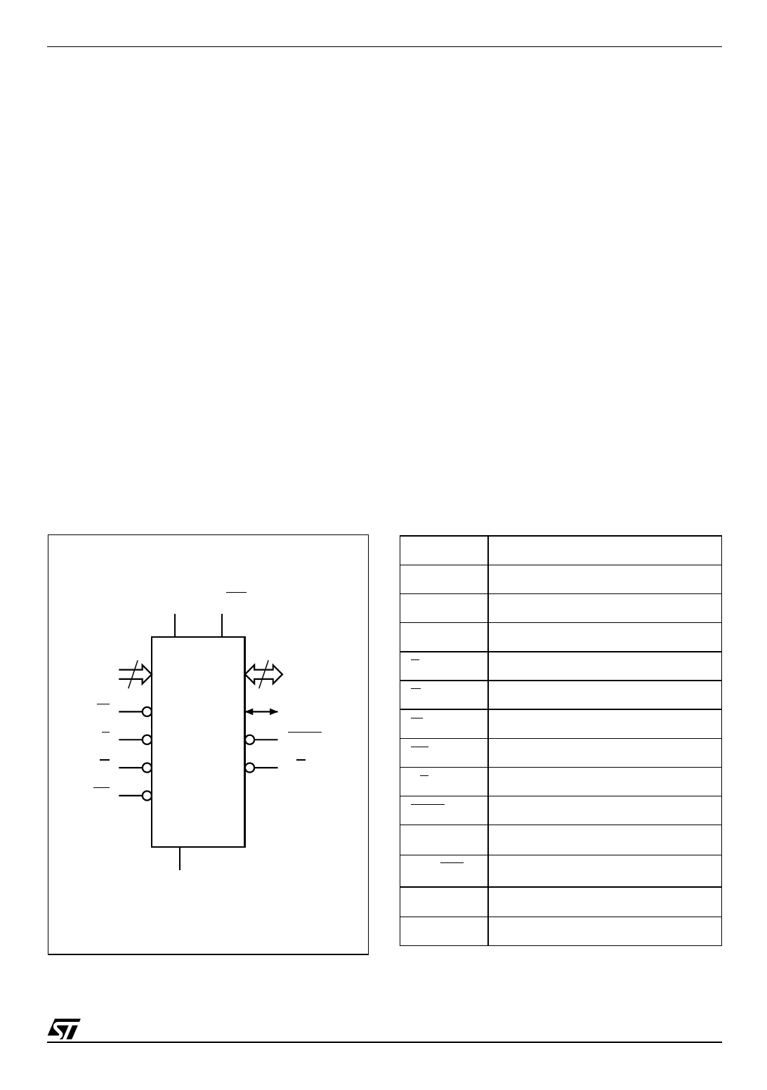
Figure 2. Logic Diagram
VCC VPP/WP
21
A0-A20
15
DQ0-DQ14
W
DQ15A–1
M29DW323DT
E
M29DW323DB
BYTE
G
RB
RP
VSS
AI05523
Table 1. Signal Names
A0-A20
Address Inputs
DQ0-DQ7 Data Inputs/Outputs
DQ8-DQ14 Data Inputs/Outputs
DQ15A–1 Data Input/Output or Address Input
E
Chip Enable
G
Output Enable
W
Write Enable
RP
Reset/Block Temporary Unprotect
RB
Ready/Busy Output
BYTE
Byte/Word Organization Select
VCC
Supply Voltage
VPP/WP
VPP/Write Protect
VSS
Ground
NC
Not Connected Internally
5/49
Share Link: