M29F002 データシートの表示(PDF) - STMicroelectronics
部品番号
コンポーネント説明
メーカー
M29F002 Datasheet PDF : 29 Pages
| |||
M29F002T, M29F002NT, M29F002B
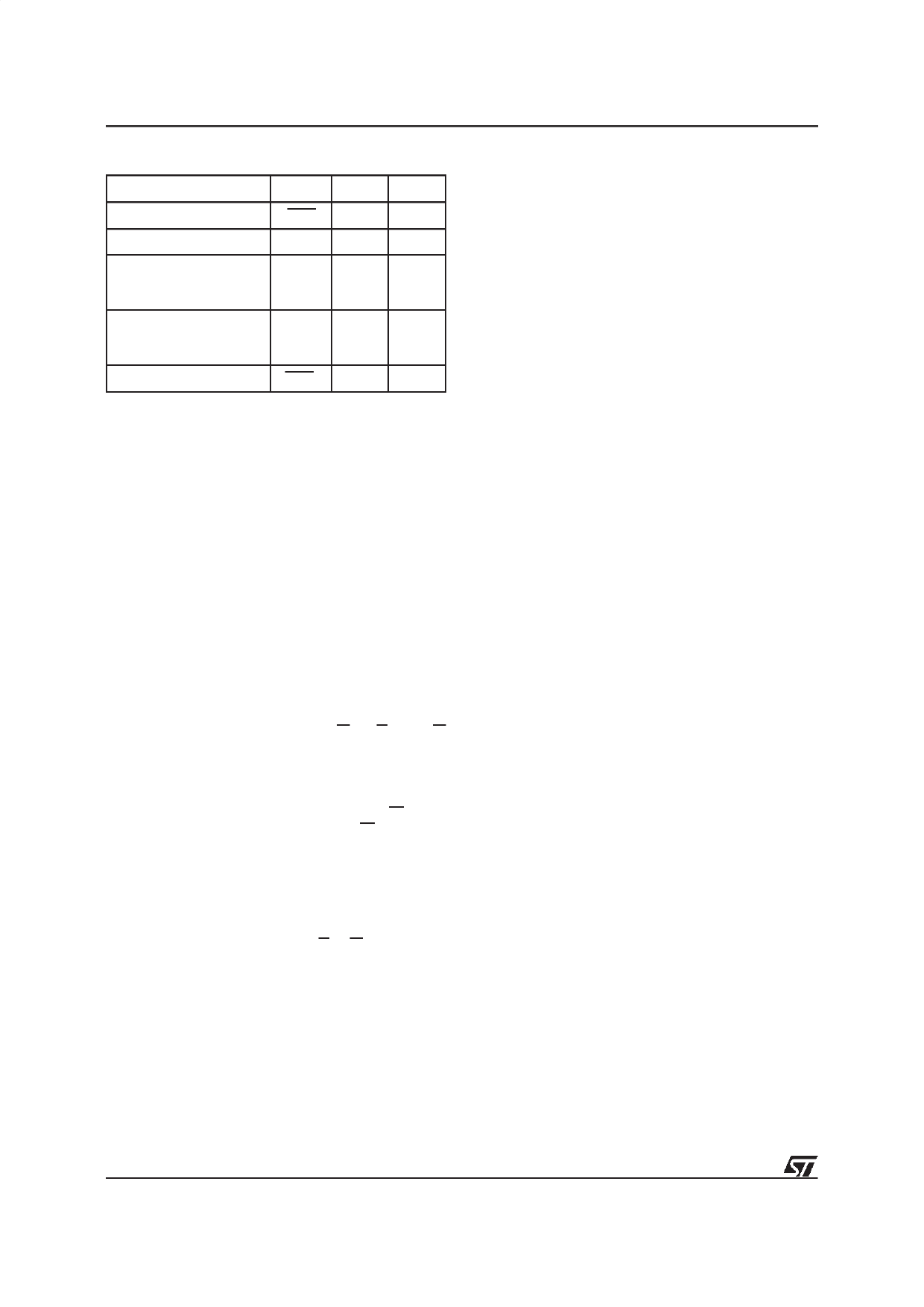
Table 10. Polling and Toggle Bits
Mode
DQ7 DQ6 DQ2
Program
DQ7 Toggle 1
Erase
Erase Suspend Read
(in Erase Suspend
block)
0
Toggle Note 1
1
1 Toggle
Erase Suspend Read
(outside Erase Suspend
block)
DQ7
DQ6
DQ2
Erase Suspend Program DQ7 Toggle N/A
Note: 1. Toggle if the address is within a block being erased.
’1’ if the address is within a block not being erased.
See Figure 11 for the Data Polling flowchart and
Figure 10 for the Data Polling waveforms. DQ7 will
also flag the Erase Suspend mode by switching
from ’0’ to ’1’ at the start of the Erase Suspend. In
order to monitor DQ7 in the Erase Suspend mode
an address within a block being erased must be
provided. For a Read Operationin Erase Suspend
mode, DQ7 will output ’1’ if the read is attempted
on a blockbeing erased and the datavalue on other
blocks. During Program operation in Erase Sus-
pend Mode, DQ7 will have the same behaviour as
in the normal program execution outside of the
suspend mode.
Toggle Bit (DQ6). When Programming or Erasing
operations are in progress, successive attempts to
read DQ6 will output complementarydata. DQ6 will
toggle following toggling of either G, or E when G
is low. The operation is completed when two suc-
cessive reads yield the same output data. The next
read will output the bit last programmed or a ’1’ after
erasing. The toggle bit DQ6 is valid only during
P/E.C. operations, that is after the fourth W pulse
for programming or after the sixth W pulse for
Erase. If the blocks selected for erasure are pro-
tected, DQ6 will toggle for about 100µs and then
return back to Read. DQ6 will be set to ’1’ if a Read
operationis attemptedon an Erase Suspendblock.
When erase is suspended DQ6 will toggle during
programming operations in a block different to the
block in Erase Suspend. Either E or G toggling will
cause DQ6 to toggle. See Figure 12 for Toggle Bit
flowchart and Figure 13 for Toggle Bit waveforms.
Toggle Bit (DQ2). This toggle bit, together with
DQ6, can be used to determine the device status
during the Erase operations. It can also be used to
identify the block being erased. During Erase or
Erase Suspend a read from a block being erased
will cause DQ2 to toggle. A read from a block not
being erased will set DQ2 to ’1’ during erase and
to DQ2 during Erase Suspend. During Chip Erase
a read operation will cause DQ2 to toggle as all
blocks are being erased. DQ2 will be set to ’1’
during program operation and when erase is com-
plete. After erase completion and if the error bit
DQ5 is set to ’1’, DQ2 will toggle if the faulty block
is addressed.
Error Bit (DQ5). This bit is set to ’1’ by the P/E.C.
when there is a failure of programming, block
erase, or chip erase that results in invalid data in
the memory block. In caseof an error in block erase
or program, the block in which the error occured or
to which the programmed data belongs, must be
discarded. The DQ5 failure condition will also ap-
pear if a user tries to program a ’1’ to a location that
is previously programmed to ’0’. Other Blocks may
stillbe used.The error bit resets after a Read/Reset
(RD) instruction. In case of success of Program or
Erase, the error bit will be set to ’0’ .
Erase Timer Bit (DQ3). This bit is set to ’0’ by the
P/E.C. when the last block Erase command has
been entered to the Command Interface and it is
awaiting the Erase start. When the erase timeout
period is finished, after 50µs to 120µs, DQ3 returns
to ’1’.
Coded Cycles
The two Coded cycles unlock the Command Inter-
face. They are followed by an input command or a
confirmation command. The Coded cycles consist
of writing the data AAh at address 555h during the
first cycle. During the second cycle the Coded
cycles consist of writing the data 55h at address
AAAh. The address lines A0 to A11 are valid, other
address lines are ’don’t care’. The Coded cycles
happen on first and second cycles of the command
write or on the fourth and fifth cycles.
Instructions
See Table 8.
Read/Reset (RD) Instruction. The Read/Reset
instruction consists of one write cycle giving the
command F0h. It canbe optionallypreceded by the
two Coded cycles. Subsequentread operationswill
read the memory array addressed and output the
data read. A wait state of 10µs is necessary after
Read/Reset prior to any valid read if the memory
was in an Erase mode when the RD instruction is
given.
10/29
Share Link: 