M29F002 データシートの表示(PDF) - STMicroelectronics
部品番号
コンポーネント説明
メーカー
M29F002 Datasheet PDF : 29 Pages
| |||
M29F002T, M29F002NT, M29F002B
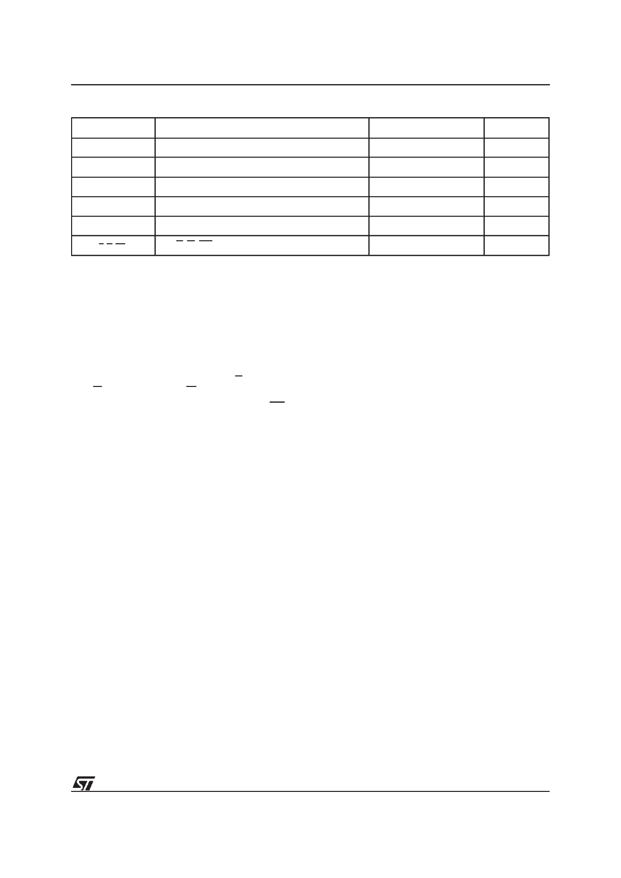
Table 2. Absolute Maximum Ratings (1)
Symbol
Parameter
Value
Unit
TA
Ambient Operating Temperature (3)
–40 to 125
°C
TBIAS
Temperature Under Bias
–50 to 125
°C
TSTG
VIO (2)
Storage Temperature
Input or Output Voltages
–65 to 150
°C
–0.6 to 7
V
VCC
Supply Voltage
–0.6 to 7
V
V(A9, E, G, RPNC) (2) A9, E, G, RPNC Voltage
–0.6 to 13.5
V
Notes: 1. Except for the rating ”Operating Temperature Range”, stresses above those listed in the Table ”Absolute Maximum Ratings”
may cause permanent damage to the device. These are stress ratings only and operation of the device at these or any other
conditions above those indicated in the Operating sections of this specification is not i mplied. Exposure to Absolute Maximum
Rating conditions for extended periods may affect device reliability. Refer also to the STMicroelectronics SURE Program and other
relevant quality documents.
2. Minimum Voltage may undershoot to –2V during transition and for less than 20ns.
3. Depends on range.
Organisation
The M29F002 is organised as 256K x 8. Memory
control is provided by Chip Enable E, Output En-
able G and Write Enable W inputs.
A Reset/Block Temporary Unprotection RPNC
(NOT available on M29F002NT) tri-level input pro-
vides a hardwarereset when pulled Low, and when
held High (at VID) temporarily unprotects blocks
previously protected allowing them to be progra-
med and erased. Erase and Program operations
are controlled by an internal Program/Erase Con-
troller (P/E.C.).StatusRegister data outputon DQ7
provides a Data Polling signal, and DQ6 and DQ2
provide Toggle signals to indicate the state of the
P/E.C operations.
Memory Blocks
The devices feature asymmetrically blocked archi-
tecture providing system memory integration. The
M29F002 has an array of 7 blocks, one Boot Block
of 16 KBytes, two Parameter Blocks of 8 KBytes,
one Main Block of 32 KBytes and three Main Blocks
of 64 KBytes.
The memory map is shown in Figure 3. Each block
can be erased separately, any combination of
blocks can be specified for multi-block erase or the
entire chip may be erased. The Erase operations
are managedautomaticallyby the P/E.C.The block
erase operation can be suspended in order to read
from or program to any block not being ersased,
and then resumed. Block protection provides addi-
tional data security. Each block can be separately
protectedor unprotectedagainstProgram or Erase
on programming equipment. All previously pro-
tected blocks can be temporarily unprotectedin the
application.
Bus Operations
The following operations can be performed using
the appropriatebus cycles: Read (Array, Electronic
Signature, Block Protection Status), Write com-
mand, Output Disable, Standby, Reset, Block Pro-
tection, Unprotection, Protection Verify,
Unprotection Verify and Block Temporary Unpro-
tection. See Tables 4 and 5.
Command Interface
Instructions, made up of commands written in cy-
cles, can be given to the Program/EraseController
through a Command Interface (C.I.). For added
data protection, program or erase execution starts
after 4 or 6 cycles. The first, second, fourth and fifth
cycles are used to input Coded cycles to the C.I.
This Coded sequence is the same for all Pro-
gram/Erase Controller instructions. The ’Com-
mand’ itself and its confirmation, when applicable,
are given on the third, fourth or sixth cycles. Any
incorrect command or any improper command se-
quence will reset the device to Read Array mode.
3/29
Share Link: 