M29F002 データシートの表示(PDF) - STMicroelectronics
部品番号
コンポーネント説明
メーカー
M29F002 Datasheet PDF : 29 Pages
| |||
M29F002T, M29F002NT, M29F002B
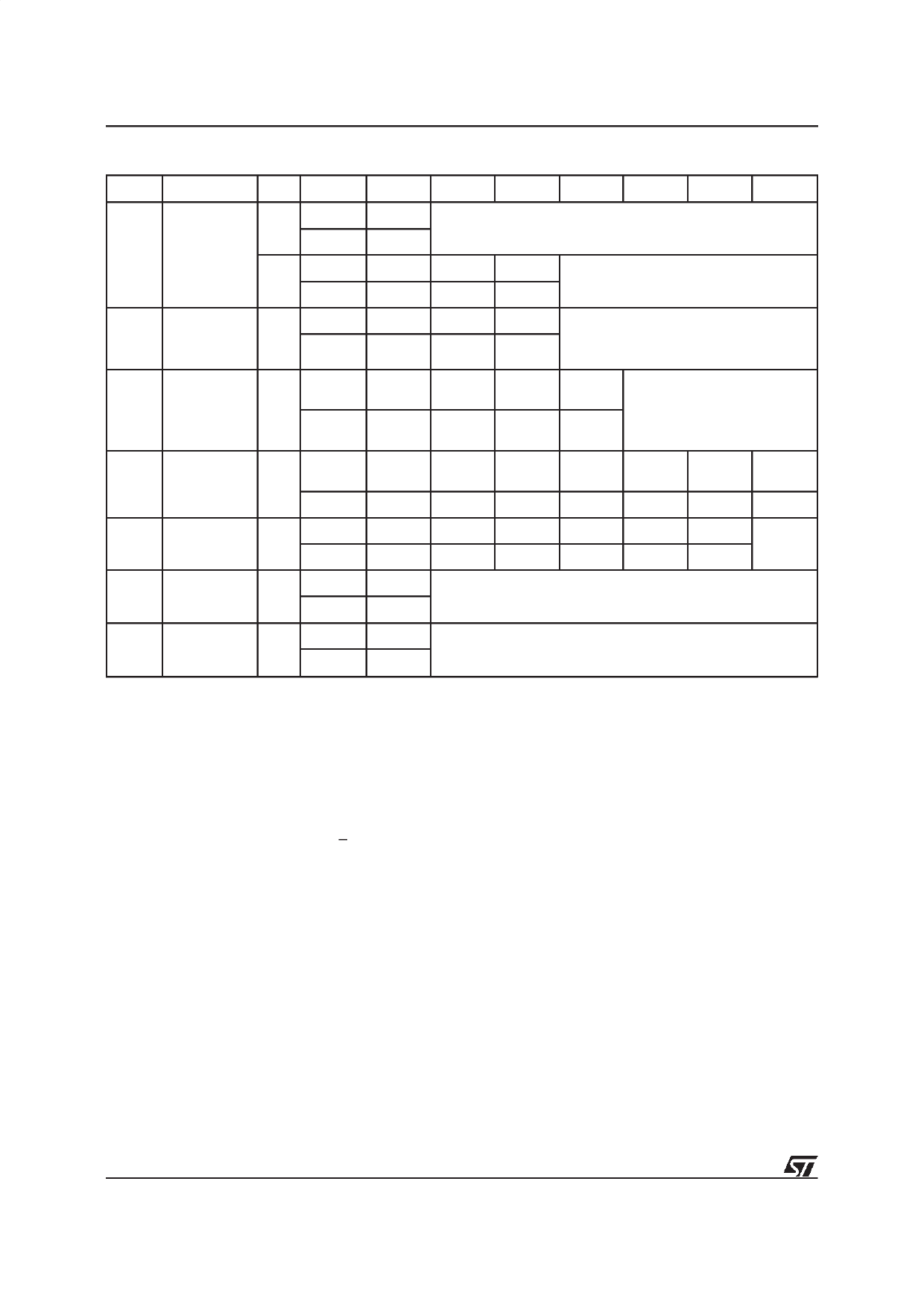
Table 8. Instructions (1)
Mne.
Instr.
Cyc.
1st Cyc. 2nd Cyc. 3rd Cyc. 4th Cyc. 5th Cyc. 6th Cyc. 7th Cyc.
RD (2,4)
Read/Reset
Memory Array
Addr. (3,7)
1+
Data
Addr. (3,7)
3+
Data
X
F0h
555h
AAh
Read Memory Array until a new write cycle is initiated.
AAAh
55h
555h
F0h
Read Memory Array until a new write
cycle is initiated.
AS (4) Auto Select
Addr. (3,7) 555h
3+
Data
AAh
AAAh
55h
555h
90h
Read Electronic Signature or Block
Protection Status until a new write cycle
is initiated. See Note 5 and 6.
PG Program
Addr. (3,7) 555h
4
Data
AAh
AAAh
55h
555h
A0h
Program
Address Read Data Polling or Toggle
Bit until Program completes.
Program
Data
BE Block Erase
Addr. (3,7) 555h
6
AAAh
555h
555h
AAAh
Block Additional
Address Block (8)
Data
AAh
55h
80h
AAh
55h
30h
30h
CE Chip Erase
Addr. (3,7) 555h
6
Data
AAh
AAAh
55h
555h
80h
555h
AAh
AAAh
55h
555h
10h
Note 9
ES (10)
Erase
Suspend
Addr. (3,7)
1
X
Read until Toggle stops, then read all the data needed from
any Block(s) not being erased then Resume Erase.
Data
B0h
ER
Erase
Resume
Addr. (3,7)
1
X
Read Data Polling or Toggle Bits until Erase completes or
Erase is suspended another time
Data
30h
Notes: 1. Commands not interpreted in this table will default to read array mode.
2. A wait of tPLYH is necessary after a Read/Reset command if the memory was in an Erase or Program mode
before starting any new operation (see Table 14 and Figure 9).
3. X = Don’t Care.
4. The first cycles of the RD or AS instructions are followed by read operations. Any number of read cycles can occur after
the command cycles.
5. Signature Address bits A0, A1 at VIL will output Manufacturer code (20h). Address bits A0 at VIH and A1 at VIL will output
Device code.
6. Block Protection Address: A0 at VIL, A1 at VIH and A13-A17 within the Block will output the Block Protection status.
7. For Coded cycles address inputs A12-A17 are don’t care.
8. Optional, additional Blocks addresses must be entered within the erase timeout delay after last write entry,
timeout status can be verified through DQ3 value (see Erase Timer Bit DQ3 description).
When full command is entered, read Data Polling or Toggle bit until Erase is completed or suspended.
9. Read Data Polling, Toggle bits or RB until Erase completes.
10.During Erase Suspend, Read and Data Program functions are allowed in blocks not being erased.
The instructions require from 1 to 6 cycles, the first
or first three of which are always write operations
used to initiate the instruction.They are followed by
either further write cycles to confirm the first com-
mand or execute the command immediately. Com-
mand sequencing must be followed exactly. Any
invalid combination of commands will reset the
device to Read Array. The increased number of
cycles has been chosen to assure maximum data
security. Instructions are initialised by two initial
Coded cycles which unlock the Command Inter-
face. In addition, for Erase, instruction confirmation
is again preceded by the two Coded cycles.
Status Register Bits
P/E.C. status is indicated during execution by Data
Polling on DQ7, detection of Toggle on DQ6 and
DQ2, or Error on DQ5 and Erase Timer DQ3 bits.
Any read attempt during Program or Erase com-
mand execution will automatically output these five
Status Register bits. The P/E.C. automatically sets
bits DQ2, DQ3, DQ5, DQ6 and DQ7. Other bits
(DQ0, DQ1 and DQ4) are reserved for future use
and should be masked. See Tables 9 and 10.
8/29
Share Link: 