M29F002 データシートの表示(PDF) - STMicroelectronics
部品番号
コンポーネント説明
メーカー
M29F002 Datasheet PDF : 29 Pages
| |||
M29F002T, M29F002NT, M29F002B
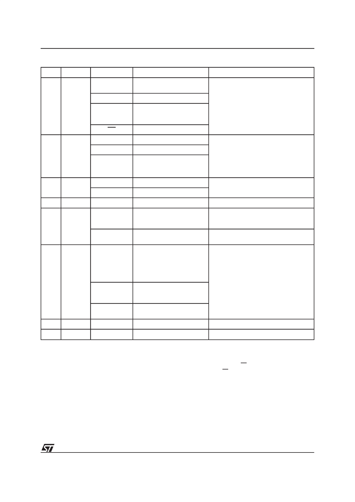
Table 9. Status Register Bits
DQ
Name
Logic Level
Definition
Note
7
Data
Polling
’1’
Erase Complete or erase
block in Erase Suspend
’0’
Erase On-going
Indicates the P/E.C. status, check during
Program or Erase, and on completion
DQ
Program Complete or data
of non erase block during
before checking bits DQ5 for Program or
Erase Success.
Erase Suspend
DQ
Program On-going
’-1-0-1-0-1-0-1-’ Erase or Program On-going
DQ
Program Complete
6 Toggle Bit
Erase Complete or Erase
’-1-1-1-1-1-1-1-’ Suspend on currently
addressed block
Successive reads output complementary
data on DQ6 while Programming or Erase
operations are on-going. DQ6 remains at
constant level when P/E.C. operations are
completed or Erase Suspend is
acknowledged.
5 Error Bit
’1’
Program or Erase Error
This bit is set to ’1’ in the case of
Programming or Erase failure.
’0’
Program or Erase On-going
4 Reserved
3
Erase
Time Bit
P/E.C. Erase operation has started. Only
’1’
Erase Timeout Period Expired possible command entry is Erase Suspend
(ES).
’0’
Erase Timeout Period
On-going
An additional block to be erased in parallel
can be entered to the P/E.C.
Chip Erase, Erase or Erase
Suspend on the currently
’-1-0-1-0-1-0-1-’
addressed block.
Erase Error due to the
currently addressed block
2 Toggle Bit
(when DQ5 = ’1’).
Indicates the erase status and allows to
identify the erased block
Program on-going, Erase
1
on-going on another block or
Erase Complete
DQ
Erase Suspend read on
non Erase Suspend block
1 Reserved
0 Reserved
Notes: Logic level ’1’ is High, ’0’ is Low. -0-1-0-0-0-1-1-1-0- represent bit value in successive Read operations.
Data Polling Bit (DQ7). When Programming op-
erations are in progress, this bit outputs the com-
plement of the bit being programmed on DQ7.
During Erase operation, it outputs a ’0’. After com-
pletion of the operation, DQ7 will output the bit last
programmed or a ’1’ after erasing. Data Polling is
valid and only effective during P/E.C. operation,
that is after the fourth W pulse for programming or
after the sixth W pulse for erase. It must be per-
formed at the address being programmed or at an
address within the block being erased. If all the
blocks selected for erasure are protected, DQ7 will
be set to ’0’ for about 100µs, and then return to the
previous addressed memory data value.
9/29
Share Link: 