M29W008EB データシートの表示(PDF) - STMicroelectronics
部品番号
コンポーネント説明
メーカー
M29W008EB Datasheet PDF : 43 Pages
| |||
2 Signal descriptions
2 Signal descriptions
M29W008ET, M29W008EB
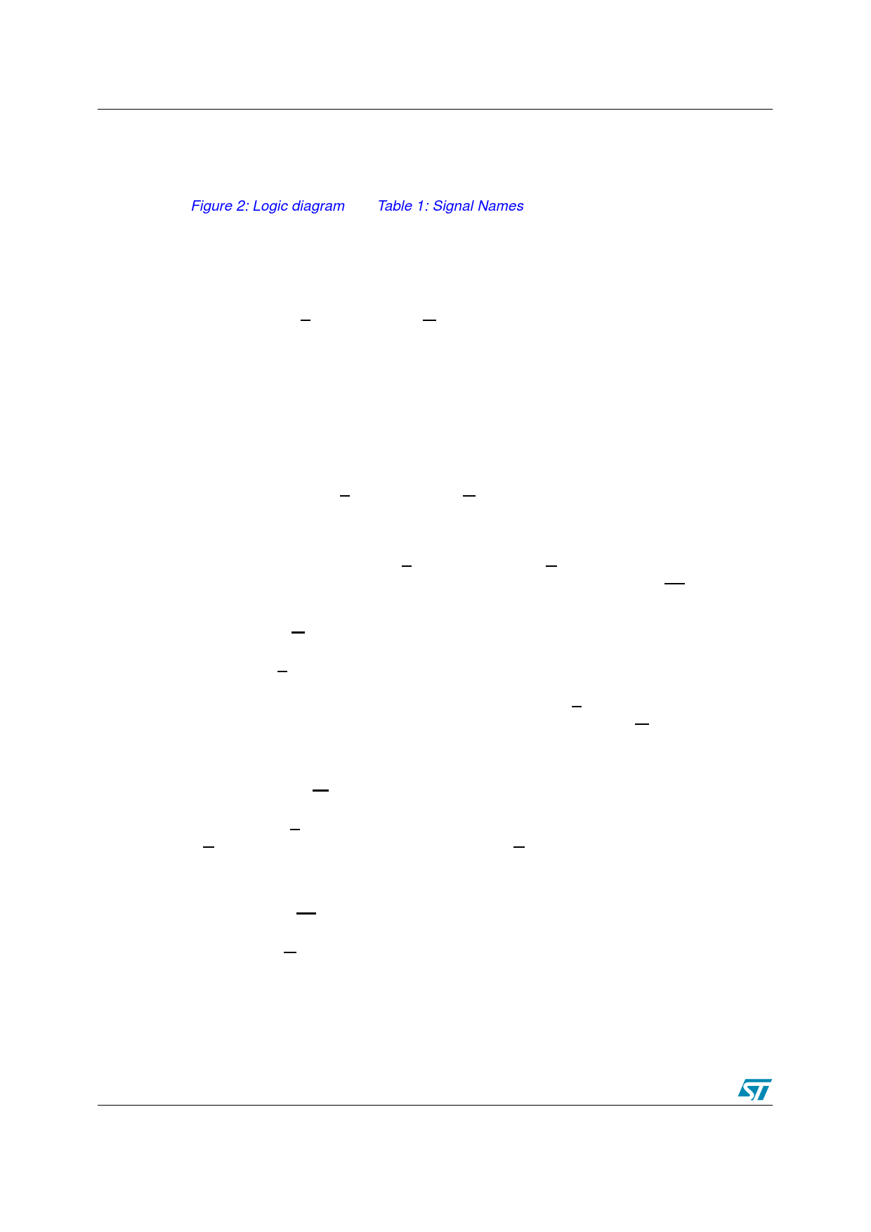
See Figure 2: Logic diagram and Table 1: Signal Names, for a brief overview of the signals
connected to this device.
2.1 Address Inputs (A0-A19)
The address inputs for the memory array are latched during a Bus Write operation on the falling
edge of Chip Enable, E or Write Enable, W. When A9 is raised to VID, either a Read Electronic
Signature Manufacturer or Device Code, Block Protection Status or a Write Block Protection or
Block Unprotection is enabled depending on the combination of levels on A0, A1 A6, A12 and
A15.
2.2 Data Input/Outputs (DQ0-DQ7)
During Bus Write operations, the Data Inputs/Outputs input the data to be programmed in the
memory array or a command to be written to the Command Interface. Both are latched on the
rising edge of Chip Enable, E or Write Enable, W. The Data Inputs/Outputs output the data
stored at the selected address during a Bus Read operation, the Electronic Signature
(Manufacturer or Device codes), the Block Protection Status or the Data Polling bit (DQ7),
Toggle Bits (DQ6) and DQ2), Error bit (DQ5) or Erase Timer bit (DQ3) of the Status Register.
Outputs are valid when Chip Enable, E and Output Enable, G are active. The output is high
impedance when the chip is deselected or the outputs are disabled and when RP is Low.
2.3 Chip Enable (E)
The Chip Enable, E, activates the memory control logic, input buffers, decoders and sense
amplifiers. When Chip Enable is High, VIH, the memory is deselected and the power
consumption is reduced to the Standby level. The Chip Enable, E, can also be used to control
Write operations to the command register and to the memory array, while W remains Low. The
Chip Enable must be forced to VID during Block Unprotection operations.
2.4 Output Enable (G)
The Output Enable, G, gates the outputs through the data buffers during a Bus Read operation.
When G is High, VIH, the outputs are high impedance. G must be forced to VID during Block
Protection and Unprotection operations.
2.5 Write Enable (W)
This Write Enable, W, controls write operations of the memory’s Command Interface.
10/43
Share Link: 