M29W008EB データシートの表示(PDF) - STMicroelectronics
部品番号
コンポーネント説明
メーカー
M29W008EB Datasheet PDF : 43 Pages
| |||

1 Summary description
1 Summary description
M29W008ET, M29W008EB
The M29W008E is a 8 Mbit (1Mb x 8) non-volatile Flash memory that can be read, erased at
block, multi-block or chip level and programmed at Byte level. These operations are performed
using a single 2.7V to 3.6V VCC supply voltage. For Program and Erase operations the
necessary high voltages are generated internally. The device can also be programmed using
standard programming equipment.
The memory is divided into blocks that are asymmetrically arranged. Both M29W008ET and
M29W008EB devices have an array of 19 blocks composed of one Boot Block of 16 KBytes,
two Parameter Blocks of 8 KBytes, one Main Block of 32 KBytes and fifteen Main Blocks of 64
KBytes. In the M29W008ET, the Boot Block is located at the top of the memory address space
while in the M29W008EB, it is located at the bottom. The memory maps are showed in
Figure 4: Block Addresses (Top Boot Block) and Figure 5: Block Addresses (Bottom Boot
Block). Each block can be erased and reprogrammed independently so it is possible to
preserve valid data while old data is erased. Program and Erase commands are written to the
Command Interface of the memory. An on-chip Program/Erase Controller simplifies the
process of programming or erasing the memory by taking care of all of the special operations
that are required to update the memory contents. The end of a program or erase operation can
be detected and any error conditions identified. Erase operations in one block can be
temporarily suspended in order to read from or program in blocks that are not being erased.
Each block can be programmed and erased over 100,000 cycles.
Each block can be protected independently to prevent accidental Program or Erase commands
from modifying the memory. All previously protected blocks can be temporarily unprotected.
In order to meet environmental requirements, ST offers this device in a TSOP40 (10 x 20mm)
ECOPACK® package. ECOPACK® packages are Lead-free and RoHS compliant. The category
of second Level Interconnect is marked on the package and on the inner box label, in
compliance with JEDEC Standard JESD97. The maximum ratings related to soldering
conditions are also marked on the inner box label. ECOPACK is an ST trademark. ECOPACK
specifications are available at: www.st.com.
The device is offered in package and supplied with all the bits erased (set to ’1’).
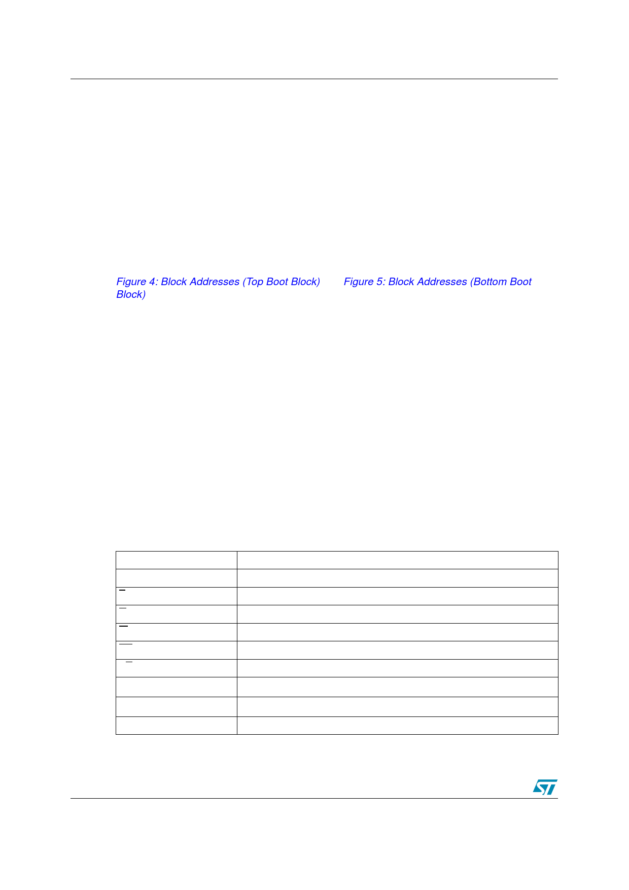
Table 1.
A0-A19
Signal Names
Address Inputs
DQ0-DQ7
Data Input/Outputs, Command Inputs
E
Chip Enable
G
Output Enable
W
Write Enable
RP
Reset/Block Temporary Unprotect
RB
Ready/Busy Output
VCC
Supply Voltage
VSS
Ground
NC
Not Connected Internally
6/43