M36W0R5020B0 データシートの表示(PDF) - STMicroelectronics
部品番号
コンポーネント説明
メーカー
M36W0R5020B0
32 Mbit (2Mb x16, Multiple Bank, Burst) Flash Memory and 4 Mbit SRAM, 1.8V Supply Multi-Chip Package
STMicroelectronics

M36W0R5020B0 Datasheet PDF : 26 Pages
| |||
M36W0R5020T0, M36W0R5020B0
SUMMARY DESCRIPTION
The M36W0R5020T0 and M36W0R5020B0 com-
bine two memory devices in a Multi-Chip Package:
■ a 32-Mbit, Multiple Bank Flash memory, the
M58WR032FT/B
■ and a 4-Mbit SRAM.
Recommended operating conditions do not allow
more than one memory to be active at the same
time.
The memory is offered in a Stacked TFBGA88
(8 x 10mm, 8x10 ball array, 0.8mm pitch) pack-
age.
In addition to the standard version, the package is
also available in Lead-free version, in compliance
with JEDEC Std J-STD-020B, the ST ECOPACK
7191395 Specification, and the RoHS (Restriction
of Hazardous Substances) directive. All packages
are compliant with Lead-free soldering processes.
The memory supplied with all the bits erased (set
to ‘1’).
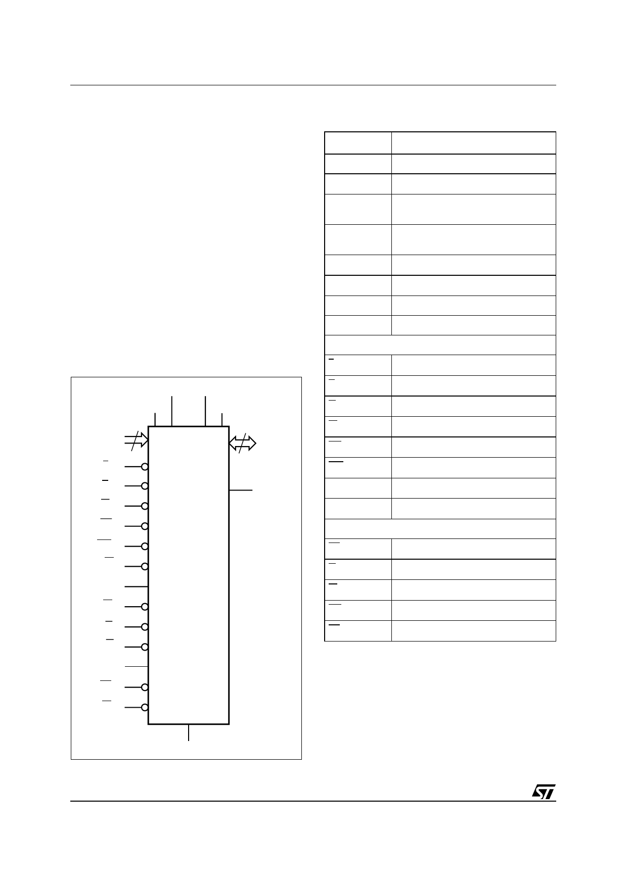
Figure 2. Logic Diagram
VDDQ
VDDF
VPPF
VDDS
21
16
A0-A20
DQ0-DQ15
EF
GF
WAITF
WF
RPF
WPF
LF
KF
M36W0R5020T
M36W0R5020B
E1S
GS
WS
E2S
UBS
LBS
Table 1. Signal Names
A0-A20 (1)
Address Inputs
DQ0-DQ15 Common Data Input/Output
VDDF
Flash Memory Power Supply
VDDQ
Common Flash and SRAM Power
Supply for I/O Buffers
VPPF
Common Flash Optional Supply
Voltage for Fast Program and Erase
VSS
Ground
VDDS
SRAM Power Supply
NC
Not Connected Internally
DU
Do Not Use as Internally Connected
Flash Memory
LF
Latch Enable input
EF
Chip Enable input
GF
Output Enable input
WF
Write Enable input
RPF
Reset input
WPF
Write Protect input
KF
Burst Clock
WAITF
Wait Data in Burst Mode
SRAM
E1S, E2S
Chip Enable input
GS
Output Enable input
WS
Write Enable input
UBS
Upper Byte Enable input
LBS
Lower Byte Enable input
Note: 1. A20-A18 are address inputs for the Flash memory com-
ponent only.
VSS
AI08754b
4/26
Share Link: