M50FW040 データシートの表示(PDF) - STMicroelectronics
部品番号
コンポーネント説明
メーカー
M50FW040 Datasheet PDF : 41 Pages
| |||
M50FW040
4 Mbit (512Kb x8, Uniform Block)
3V Supply Firmware Hub Flash Memory
FEATURES SUMMARY
■ SUPPLY VOLTAGE
– VCC = 3V to 3.6V for Program, Erase and
Read Operations
– VPP = 12V for Fast Erase (optional)
■ TWO INTERFACES
– Firmware Hub (FWH) Interface for
embedded operation with PC Chipsets.
– Address/Address Multiplexed (A/A Mux)
Interface for programming equipment
compatibility.
■ FIRMWARE HUB (FWH) HARDWARE
INTERFACE MODE
– 5 Signal Communication Interface
supporting Read and Write Operations
– Hardware Write Protect Pins for Block
Protection
– Register Based Read and Write
Protection
– 5 Additional General Purpose Inputs for
platform design flexibility
– Synchronized with 33MHz PCI clock
■ PROGRAMMING TIME: 10µs typical
■ 8 UNIFORM 64 Kbyte MEMORY BLOCKS
■ PROGRAM/ERASE CONTROLLER
– Embedded Byte Program and Block
Erase algorithms
– Status Register Bits
■ PROGRAM and ERASE SUSPEND
– Read other Blocks during Program/Erase
Suspend
– Program other Blocks during Erase
Suspend
■ FOR USE in PC BIOS APPLICATIONS
■ ELECTRONIC SIGNATURE
– Manufacturer Code: 20h
– Device Code: 2Ch
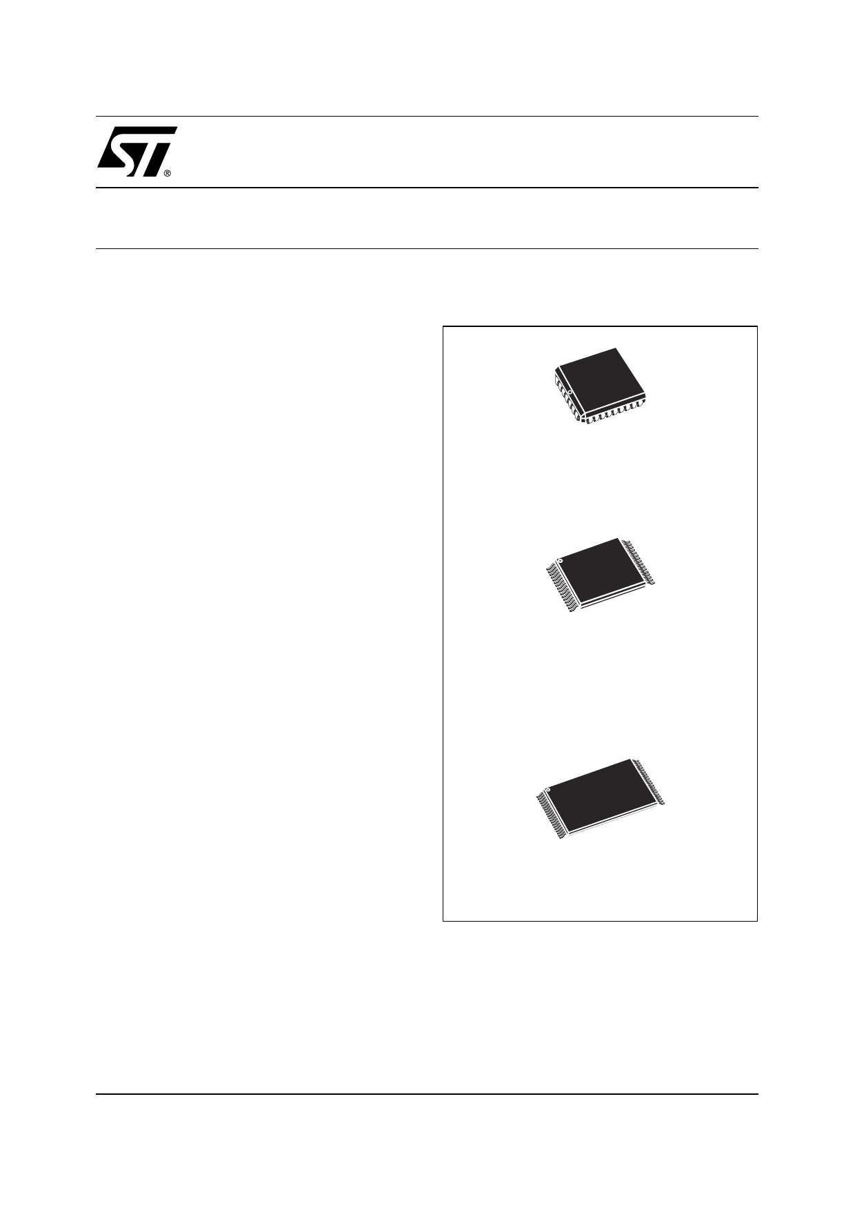
Figure 1. Packages
PLCC32 (K)
TSOP32 (NB)
8 x 14mm
TSOP40 (N)
10 x 20mm
November 2004
1/41
Share Link: 