M50LPW002 データシートの表示(PDF) - STMicroelectronics
部品番号
コンポーネント説明
メーカー
M50LPW002 Datasheet PDF : 39 Pages
| |||
M50LPW002
SUMMARY DESCRIPTION
The M50LPW002 is a 2 Mbit (256Kb x8) non-vola-
tile memory that can be read, erased and repro-
grammed. These operations can be performed
using a single low voltage (3.0 to 3.6V) supply. For
fast programming and fast erasing in production
lines an optional 12V power supply can be used to
reduce the programming and the erasing times.
The memory is divided into blocks that can be
erased independently so it is possible to preserve
valid data while old data is erased. Blocks can be
protected individually to prevent accidental Pro-
gram or Erase commands from modifying the
memory. Program and Erase commands are writ-
ten to the Command Interface of the memory. An
on-chip Program/Erase Controller simplifies the
process of programming or erasing the memory by
taking care of all of the special operations that are
required to update the memory contents. The end
of a program or erase operation can be detected
and any error conditions identified. The command
set required to control the memory is consistent
with JEDEC standards.
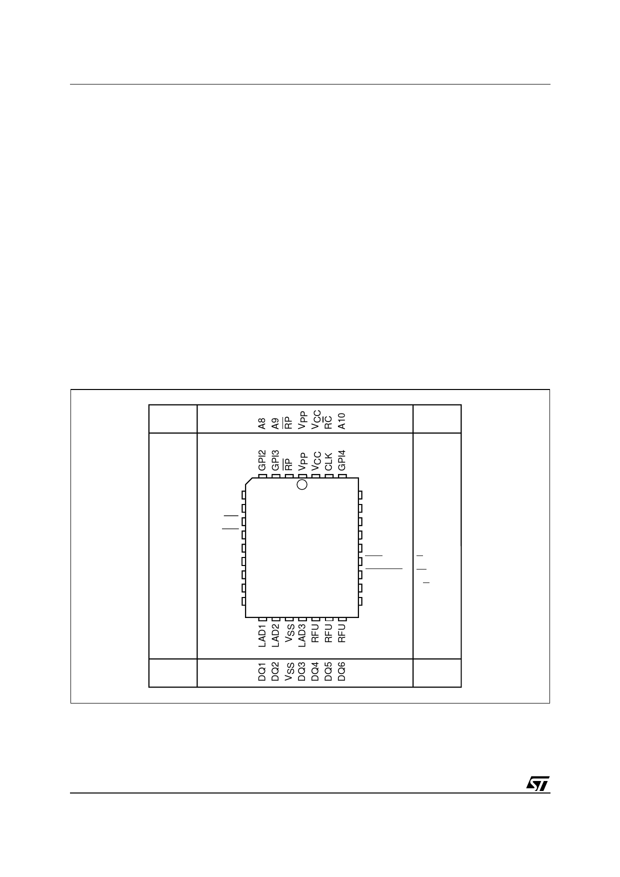
Figure 2. PLCC Connections
The device features an asymmetrical blocked ar-
chitecture. The device has an array of 7 blocks:
s 1 Boot Block of 16 KByte
s 2 Parameter Blocks of 8 KByte each
s 1 Main Block of 32 KByte
s 3 Main Blocks of 64 KByte each
Two different bus interfaces are supported by the
memory. The primary interface is the Low Pin
Count (or LPC) Standard Interface. This has been
designed to remove the need for the ISA bus in
current PC Chipsets; the M50LPW002 acts as the
PC BIOS on the Low Pin Count bus for these PC
Chipsets.
The secondary interface, the Address/Address
Multiplexed (or A/A Mux) Interface, is designed to
be compatible with current Flash Programmers for
production line programming prior to fitting to a PC
Motherboard.
The memory is delivered with all the bits erased
(set to 1).
A/A Mux
A/A Mux
A7
A6
A5
A4
A3
A2
A1
A0
DQ0
GPI1
GPI0
WP
TBL
ID3 9
ID2
ID1
ID0
LAD0
1 32
M50LPW002
17
IC (VIL)
NC
NC
VSS
25 VCC
INIT
LFRAME
RFU
RFU
IC (VIH)
NC
NC
VSS
VCC
G
W
RB
DQ7
A/A Mux
Note: Pins 27 and 28 are not internally connected.
A/A Mux
AI05744
4/39
Share Link: 