M50LPW012 データシートの表示(PDF) - STMicroelectronics
部品番号
コンポーネント説明
メーカー
M50LPW012 Datasheet PDF : 35 Pages
| |||
M50LPW012
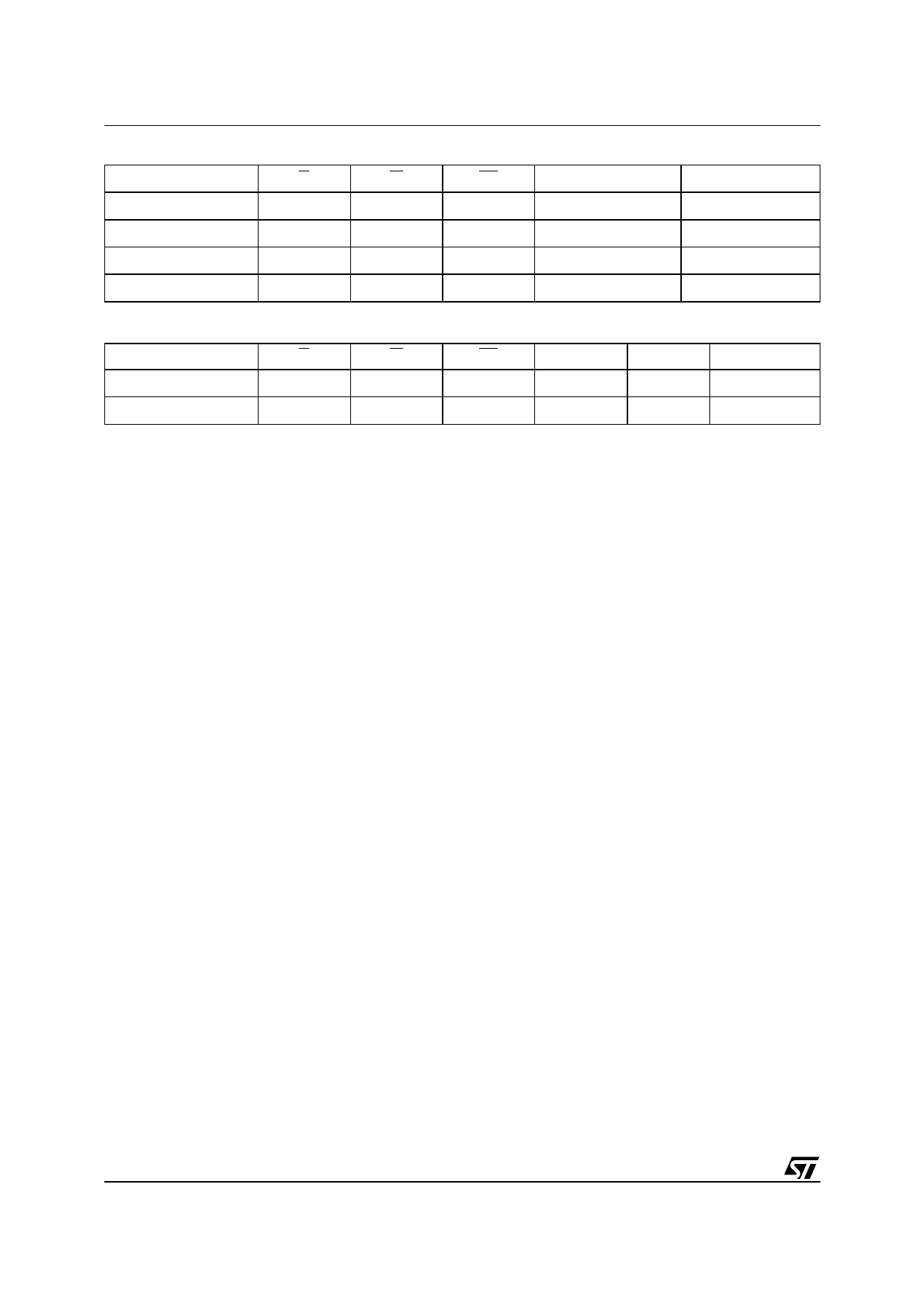
Table 9. A/A Mux Bus Operations
Operation
G
Bus Read
VIL
Bus Write
VIH
Output Disable
VIH
Reset
VIL or VIH
W
VIH
VIL
VIH
VIL or VIH
Table 10. Manufacturer and Device Codes
Operation
G
W
Manufacturer Code
VIL
VIH
Device Code
VIL
VIH
RP
VPP
DQ7-DQ0
VIH
Don’t Care
Data Output
VIH
Float or VCC or VPPH
Data Input
VIH
Don’t Care
Hi-Z
VIL
Don’t Care
Hi-Z
RP
A18-A1
A0
DQ7-DQ0
VIH
VIL
VIL
20h
VIH
VIL
VIH
3Bh
COMMAND INTERFACE
All Bus Write operations to the memory are
interpreted by the Command Interface.
Commands consist of one or more sequential Bus
Write operations.
After power-up or a Reset operation the memory
enters Read mode.
The commands are summarized in Table 12,
Commands. Refer to Table 12 in conjunction with
the text descriptions below.
Read Memory Array Command. The Read Mem-
ory Array command returns the memory to its
Read mode where it behaves like a ROM or
EPROM. One Bus Write cycle is required to issue
the Read Memory Array command and return the
memory to Read mode. Once the command is is-
sued the memory remains in Read mode until an-
other command is issued. From Read mode Bus
Read operations will access the memory array.
While the Program/Erase Controller is executing a
Program or Erase operation the memory will not
accept the Read Memory Array command until the
operation completes.
Read Status Register Command. The Read Sta-
tus Register command is used to read the Status
Register. One Bus Write cycle is required to issue
the Read Status Register command. Once the
command is issued subsequent Bus Read opera-
tions read the Status Register until another com-
mand is issued. See the section on the Status
Register for details on the definitions of the Status
Register bits.
Read Electronic Signature Command. The Read
Electronic Signature command is used to read the
Manufacturer Code and the Device Code. One
Bus Write cycle is required to issue the Read
Electronic Signature command. Once the
command is issued subsequent Bus Read
operations read the Manufacturer Code or the
Device Code until another command is issued.
After the Read Electronic Signature Command is
issued the Manufacturer Code and Device Code
can be read using Bus Read operations using the
addresses in Table 11.
Program Command. The Program command
can be used to program a value to one address in
the memory array at a time. Two Bus Write
operations are required to issue the command; the
second Bus Write cycle latches the address and
data in the internal state machine and starts the
Program/Erase Controller. Once the command is
issued subsequent Bus Read operations read the
Status Register. See the section on the Status
Register for details on the definitions of the Status
Register bits.
If the address falls in a protected block then the
Program operation will abort, the data in the
memory array will not be changed and the Status
Register will output the error.
During the Program operation the memory will
only accept the Read Status Register command
and the Program/Erase Suspend command. All
other commands will be ignored. Typical Program
times are given in Table 13.
Note that the Program command cannot change a
bit set at ‘0’ back to ‘1’ and attempting to do so will
not cause any modification on its value. One of the
Erase commands must be used to set all of the
bits in the block to ‘1’.
See Figure 13, Program Flowchart and Pseudo
Code, for a suggested flowchart on using the
Program command.
10/35
Share Link: 