M50LPW012 データシートの表示(PDF) - STMicroelectronics
部品番号
コンポーネント説明
メーカー
M50LPW012 Datasheet PDF : 35 Pages
| |||
M50LPW012
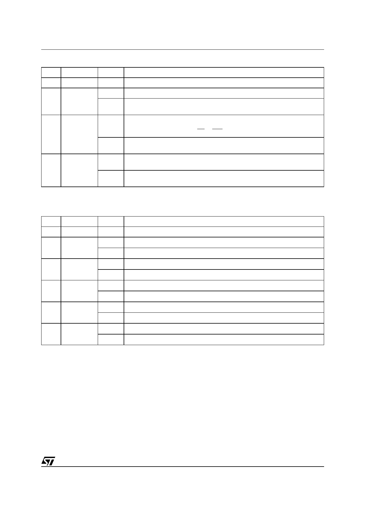
Table 16. Lock Register Bit Definitions(1)
Bit Bit Name Value
Function
7-3
Reserved
2
Read-Lock
‘1’ Bus Read operations in this Block always return 00h.
‘0’
Bus read operations in this Block return the Memory Array contents. (Default
value).
1 Lock-Down
Changes to the Read-Lock bit and the Write-Lock bit cannot be performed. Once a
‘1’ ‘1’ is written to the Lock-Down bit it cannot be cleared to ‘0’; the bit is always reset
to ‘0’ following a Reset (using RP or INIT) or after power-up.
‘0’
Read-Lock and Write-Lock can be changed by writing new values to them. (Default
value).
0
Write-Lock
‘1’
Program and Block Erase operations in this Block will set an error in the Status
Register. The memory contents will not be changed. (Default value).
‘0’
Program and Block Erase operations in this Block are executed and will modify the
Block contents.
Note: 1. Applies to Top Block Lock Register (T_BLOCK_LK) and Top Block [-1] Lock Register (T_MINUS01_LK) to Top Block [-6] Lock Reg-
ister (T_MINUS06_LK).
Table 17. General Purpose Input Register Definition(1)
Bit Bit Name Value
7-5
Reserved
4
GPI4
‘1’ Input Pin GPI4 is at VIH
‘0’ Input Pin GPI4 is at VIL
3
GPI3
‘1’ Input Pin GPI3 is at VIH
‘0’ Input Pin GPI3 is at VIL
2
GPI2
‘1’ Input Pin GPI2 is at VIH
‘0’ Input Pin GPI2 is at VIL
1
GPI1
‘1’ Input Pin GPI1 is at VIH
‘0’ Input Pin GPI1 is at VIL
0
GPI0
‘1’ Input Pin GPI0 is at VIH
‘0’ Input Pin GPI0 is at VIL
Note: 1. Applies to the General Purpose Input Register (GPI_REG).
Function
17/35
Share Link: 