M50LPW041N データシートの表示(PDF) - STMicroelectronics
部品番号
コンポーネント説明
メーカー
M50LPW041N Datasheet PDF : 37 Pages
| |||
M50LPW041
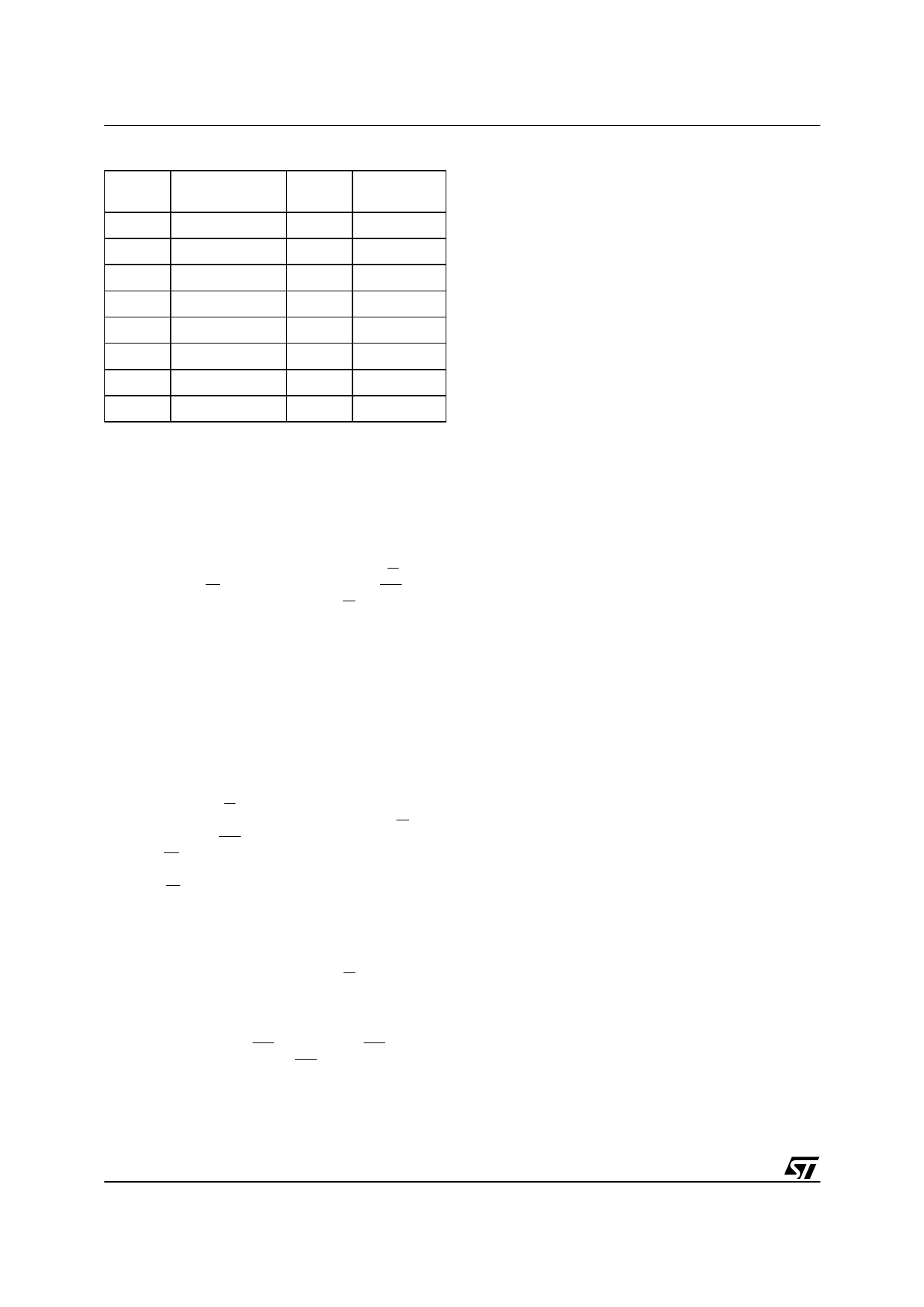
Table 6. Block Addresses
Size
(Kbytes)
Address Range
Block
Number
64 70000h-7FFFFh
7
64 60000h-6FFFFh
6
64 50000h-5FFFFh
5
64 40000h-4FFFFh
4
64 30000h-3FFFFh
3
64 20000h-2FFFFh
2
64 10000h-1FFFFh
1
64 00000h-0FFFFh
0
Note: For A19 value, refer to Table 2.
Block Type
Top Block
Main Block
Main Block
Main Block
Main Block
Main Block
Main Block
Main Block
Bus Read. Bus Read operations are used to
output the contents of the Memory Array, the
Electronic Signature and the Status Register. A
valid Bus Read operation begins by latching the
Row Address and Column Address signals into
the memory using the Address Inputs, A0-A10,
and the Row/Column Address Select RC. Then
Write Enable (W) and Interface Reset (RP) must
be High, VIH, and Output Enable, G, Low, VIL, in
order to perform a Bus Read operation. The Data
Inputs/Outputs will output the value, see Figure
12, A/A Mux Interface Read AC Waveforms, and
Table 25, A/A Mux Interface Read AC
Characteristics, for details of when the output
becomes valid.
Bus Write. Bus Write operations write to the
Command Interface. A valid Bus Write operation
begins by latching the Row Address and Column
Address signals into the memory using the
Address Inputs, A0-A10, and the Row/Column
Address Select RC. The data should be set up on
the Data Inputs/Outputs; Output Enable, G, and
Interface Reset, RP, must be High, VIH and Write
Enable, W, must be Low, VIL. The Data Inputs/
Outputs are latched on the rising edge of Write
Enable, W. See Figure 13, A/A Mux Interface
Write AC Waveforms, and Table 26, A/A Mux
Interface Write AC Characteristics, for details of
the timing requirements.
Output Disable. The data outputs are high-im-
pedance when the Output Enable, G, is at VIH.
Reset. During Reset mode all internal circuits are
switched off, the memory is deselected and the
outputs are put in high-impedance. The memory is
in Reset mode when RP is Low, VIL. RP must be
held Low, VIL for tPLPH. If RP is goes Low, VIL,
during a Program or Erase operation, the
operation is aborted and the memory cells affected
no longer contain valid data; the memory can take
up to tPLRH to abort a Program or Erase operation.
COMMAND INTERFACE
All Bus Write operations to the memory are
interpreted by the Command Interface.
Commands consist of one or more sequential Bus
Write operations.
After power-up or a Reset operation the memory
enters Read mode.
The commands are summarized in Table 12,
Commands. Refer to Table 12 in conjunction with
the text descriptions below.
Read Memory Array Command. The Read Mem-
ory Array command returns the memory to its
Read mode where it behaves like a ROM or
EPROM. One Bus Write cycle is required to issue
the Read Memory Array command and return the
memory to Read mode. Once the command is is-
sued the memory remains in Read mode until an-
other command is issued. From Read mode Bus
Read operations will access the memory array.
While the Program/Erase Controller is executing a
Program or Erase operation the memory will not
accept the Read Memory Array command until the
operation completes.
Read Status Register Command. The Read Sta-
tus Register command is used to read the Status
Register. One Bus Write cycle is required to issue
the Read Status Register command. Once the
command is issued subsequent Bus Read opera-
tions read the Status Register until another com-
mand is issued. See the section on the Status
Register for details on the definitions of the Status
Register bits.
Read Electronic Signature Command. The Read
Electronic Signature command is used to read the
Manufacturer Code and the Device Code. One
Bus Write cycle is required to issue the Read
Electronic Signature command. Once the
command is issued subsequent Bus Read
operations read the Manufacturer Code or the
Device Code until another command is issued.
After the Read Electronic Signature Command is
issued the Manufacturer Code and Device Code
can be read using Bus Read operations using the
addresses in Table 11.
Program Command. The Program command
can be used to program a value to one address in
the memory array at a time. Two Bus Write
operations are required to issue the command; the
second Bus Write cycle latches the address and
data in the internal state machine and starts the
Program/Erase Controller. Once the command is
issued subsequent Bus Read operations read the
Status Register. See the section on the Status
8/37
Share Link: 