M50LPW080 データシートの表示(PDF) - STMicroelectronics
部品番号
コンポーネント説明
メーカー
M50LPW080 Datasheet PDF : 44 Pages
| |||
M50LPW080
Table 7. LPC Bus Read Field Definitions
Clock Clock
Cycle Cycle
Number Count
Field
LAD0-
LAD3
Memory
I/O
Description
On the rising edge of CLK with LFRAME Low, the contents
1
1
START
0000b
I
of LAD0-LAD3 must be 0000b to indicate the start of a
LPC cycle.
2
1
CYCTYPE
+ DIR
010Xb
Indicates the type of cycle. Bits 3:2 must be 01b. Bit 1
I
indicates the direction of transfer: 0b for read. Bit 0 is don’t
care (X).
3-10
8
ADDR
XXXX
A 32-bit address phase is transferred starting with the most
I
significant nibble first. A23-A31 must be set to 1. A22 = 1
for Array, A22 = 0 for registers access. For A20-A21
values, see Table 3..
11
1
TAR
1111b
I
The host drives LAD0-LAD3 to 1111b to indicate a
turnaround cycle.
12
1
TAR
1111b
(float)
O
The LPC Flash Memory takes control of LAD0-LAD3
during this cycle.
13-14
2
WSYNC
0101b
The LPC Flash Memory drives LAD0-LAD3 to 0101b
O
(short wait-sync) for two clock cycles, indicating that the
data is not yet available. Two wait-states are always
included.
The LPC Flash Memory drives LAD0-LAD3 to 0000b,
15
1
RSYNC
0000b
O indicating that data will be available during the next clock
cycle.
16-17
2
DATA
XXXX
O
Data transfer is two CLK cycles, starting with the least
significant nibble.
18
1
TAR
1111b
O
The LPC Flash Memory drives LAD0-LAD3 to 1111b to
indicate a turnaround cycle.
19
1
TAR
1111b
(float)
N/A
The LPC Flash Memory floats its outputs, the host takes
control of LAD0-LAD3.
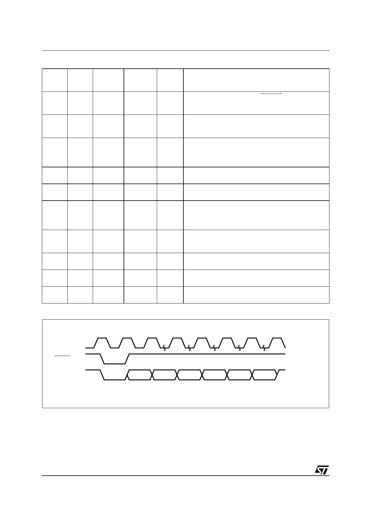
Figure 6. LPC Bus Read Waveforms
CLK
LFRAME
LAD0-LAD3
Number of
clock cycles
START
1
CYCTYPE
+ DIR
1
ADDR
8
TAR
2
SYNC
3
DATA
2
TAR
2
AI04429
14/44
Share Link: 