M58MR032-ZCT データシートの表示(PDF) - STMicroelectronics
部品番号
コンポーネント説明
メーカー
M58MR032-ZCT Datasheet PDF : 52 Pages
| |||
M58MR032C, M58MR032D
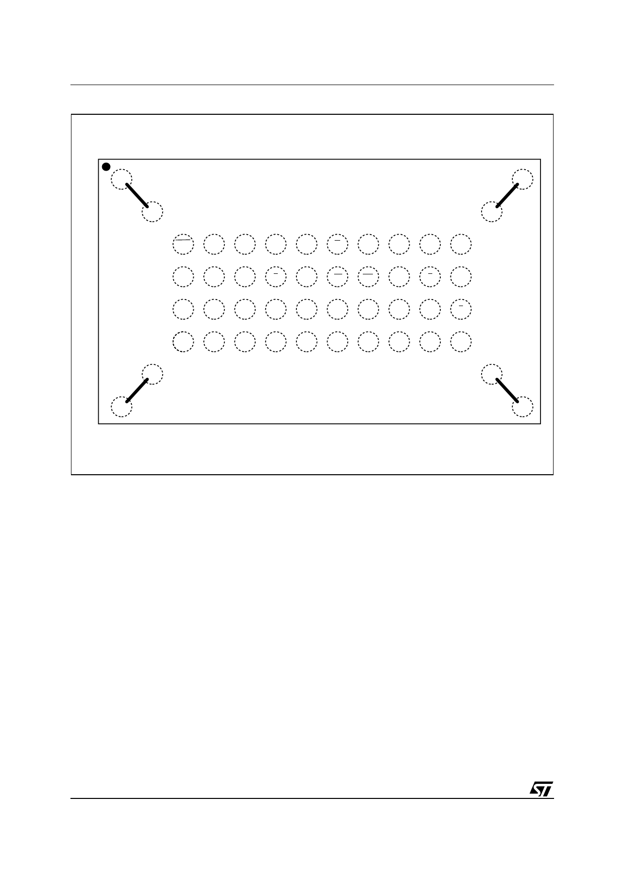
Figure 2. TFBGA Connections (Top view through package)
1
2
3
4
5
6
7
8
9
10
11
12
13
14
A
DU
B
DU
DU
DU
C
WAIT
NC
VSS
K
VDD
W
VPP
A19
A17
NC
D
VDDQ
A16
A20
L
BINV
RP
WP
A18
E
VSS
E
VSS
ADQ7 ADQ6 ADQ13 ADQ12 ADQ3 ADQ2 ADQ9 ADQ8
G
F
ADQ15 ADQ14
VSS
ADQ5
ADQ4 ADQ11 ADQ10 VDDQ
ADQ1
ADQ0
G
DU
DU
H
DU
DU
AI90020
DESCRIPTION
The M58MR032 is a 32 Mbit non-volatile Flash
memory that may be erased electrically at block
level and programmed in-system on a Word-by-
Word basis using a 1.7V to 2.0V VDD supply for the
circuitry. For Program and Erase operations the
necessary high voltages are generated internally.
The device supports synchronous burst read and
asynchronous read from all the blocks of the mem-
ory array; at power-up the device is configured for
page mode read. In synchronous burst mode, a
new data is output at each clock cycle for frequen-
cies up to 40MHz.
The array matrix organization allows each block to
be erased and reprogrammed without affecting
other blocks. All blocks are protected against pro-
gramming and erase at Power-up.
Blocks can be unprotected to make changes in the
application and then re-protected.
A parameter block "Security block" can be perma-
nently protected against programming and erasing
in order to increase the data security. An optional
12V VPP power supply is provided to speed up the
program phase at costumer production. An inter-
nal command interface (C.I.) decodes the instruc-
tions to access/modify the memory content. The
program/erase controller (P/E.C.) automatically
executes the algorithms taking care of the timings
necessary for program and erase operations. Two
status registers indicate the state of each bank.
Instructions for Read Array, Read Electronic Sig-
nature, Read Status Register, Clear Status Regis-
ter, Write Read Configuration Register, Program,
Block Erase, Bank Erase, Program Suspend, Pro-
gram Resume, Erase Suspend, Erase Resume,
Block Protect, Block Unprotect, Block Locking,
Protection Program, CFI Query, are written to the
memory through a Command Interface (C.I.) using
standard micro-processor write timings.
The memory is offered in TFBGA48, 0.5 mm ball
pitch packages and it is supplied with all the bits
erased (set to ’1’).
2/52
Share Link: 