M58MR032-ZCT データシートの表示(PDF) - STMicroelectronics
部品番号
コンポーネント説明
メーカー
M58MR032-ZCT Datasheet PDF : 52 Pages
| |||
M58MR032C, M58MR032D
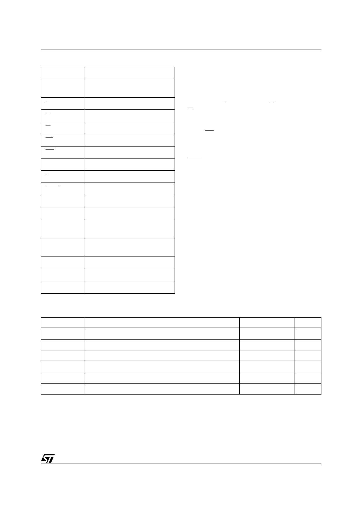
Table 1. Signal Names
A16-A20
Address Inputs
ADQ0-ADQ15
Data Input/Outputs or Address
Inputs, Command Inputs
E
Chip Enable
G
Output Enable
W
Write Enable
RP
Reset/Power-down
WP
Write Protect
K
Burst Clock
L
Latch Enable
WAIT
Wait Data in Burst Mode
BINV
Bus Invert
VDD
Supply Voltage
VDDQ
Supply Voltage for Input/Output
Buffers
VPP
Optional Supply Voltage for
Fast Program & Erase
VSS
Ground
DU
Don’t Use as Internally Connected
NC
Not Connected Internally
Table 2. Absolute Maximum Ratings (1)
Organization
The M58MR032 is organized as 2Mb by 16 bits.
The first sixteen address lines are multiplexed with
the Data Input/Output signals on the multiplexed
address/data bus ADQ0-ADQ15. The remaining
address lines A16-A20 are the MSB addresses.
Chip Enable E, Output Enable G and Write Enable
W inputs provide memory control.
The clock K input synchronizes the memory to the
microprocessor during burst read.
Reset RP is used to reset all the memory circuitry
and to set the chip in power-down mode if a proper
setting of the Read Configuration Register en-
ables this function.
WAIT output indicates to the microprocessor the
status of the memory during the burst mode oper-
ations.
Memory Blocks
The device features asymmetrically blocked archi-
tecture. M58MR032 has an array of 71 blocks and
is divided into two banks A and B, providing Dual
Bank operations. While programming or erasing in
Bank A, read operations are possible into Bank B
or vice versa. Only one bank at the time is allowed
to be in program or erase mode. It is possible to
perform burst reads that cross bank boundaries.
The memory features an erase suspend allowing
reading or programming in another block. Once
suspended the erase can be resumed. Program
can be suspended to read data in another block
and then resumed. The Bank Size and sectoriza-
tion are summarized in Table 3. Parameter Blocks
are located at the top of the memory address
space for the M58MR032C, and at the bottom for
the M58MR032D. The memory maps are shown in
Figure 3.
Symbol
Parameter
Value
Unit
TA
Ambient Operating Temperature (2)
–40 to 85
°C
TBIAS
Temperature Under Bias
–40 to 125
°C
TSTG
Storage Temperature
–55 to 155
°C
VIO (3)
Input or Output Voltage
–0.5 to VDDQ+0.5
V
VDD, VDDQ Supply Voltage
–0.5 to 2.7
V
VPP
Program Voltage
–0.5 to 13
V
Note: 1. Except for the rating "Operating Temperature Range", stresses above those listed in the Table "Absolute Maximum Ratings" may
cause permanent damage to the device. These are stress ratings only and operation of the device at these or any other conditions
above those indicated in the Operating sections of this specification is not implied. Exposure to Absolute Maximum Rating condi-
tions for extended periods may affect device reliability. Refer also to the STMicroelectronics SURE Program and other relevant qual-
ity documents.
2. Depends on range.
3. Minimum Voltage may undershoot to –2V during transition and for less than 20ns.
3/52
Share Link: 