M5913B1 データシートの表示(PDF) - STMicroelectronics
部品番号
コンポーネント説明
メーカー
M5913B1 Datasheet PDF : 17 Pages
| |||
M5913
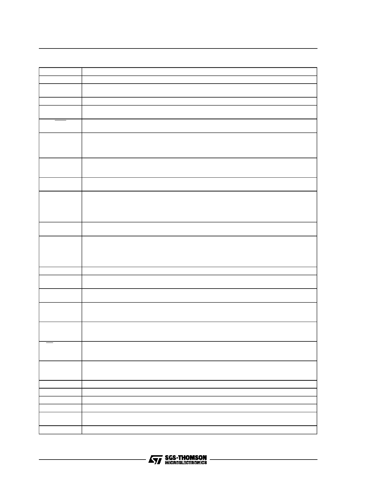
PIN DESCRIPTION
Symbol
VBB
PWRO+
PWRO -
GSR
PDN
CLKSEL
LOOP
SIGR
DCLKR
DR
FSR
GRDD
CLKR
CLKX
FSX
DX
TSX/DCLKX
SIGX/ASEL
NC
GRDA
VFXI+
VFXI-
GSX
VCC
Fu nction
Most Negative Supply. Input voltage is -5 volts ±5%.
Non-inverting Output of Power Amplifier. Can drive transformer hybrids or high impedance loads
directly in either a differential or single ended configuration.
Inverting Output of Power Amplifier. Functionally identical and complementary to PWRO+.
Input to the gain Setting Network on the Output Power Amplifier, Transmission level can be
adjusted over a 12dB range depending on the voltage at GSR.
Power Down Select. When PDN is TTL high, the device is active.When low, the device is powered
down.
input which must be pinstrapped to reflect the master clock frequency at CLKX, CLKR.
CLKSEL = VBB
2.048MHz
CLKSEL = GRDD
1.544MHz
CLKSEL = VCC
1.536MHz
Analog Loopback. When this pin is TTL high, the receive output (PWRO+) is internally connected
to VFXI+, GSR is internally connected to PWRO-, and VFXI- is internally connected to GSX.
A 0dBm0 digital signal input at DR is returned as a +3dBm0 digital signal output at DX.
Signalling Bit Output, Receive Channel. In fixed data rate mode. SIGR outputs the logical state of
the eighth bit of the PCM word in the most recent signaling frame.
Selects the fixed or variable data rate mode. When DCLKR is connected to VBB, the fixed data rate
mode is selected.
When DCLKR is not connected to VBB, the device operates in the variable data rate mode. In this
mode DCLKR becomes the receive data clock wich operates at TTL levels from 64kB to 4.096MB
data rates
Receive PCM Input. PCM data is clocked in on this lead on eight consecutive negative transitions
of the receive data clock: CLKR in the fixed data rate mode and DCLKR in variable data rate mode.
8kHz frame synchronization clock input/timeslot enable, receive channel. A multifunction input
which in fixed data rate mode distinguishes between signaling and non-signaling frames by means
of a double or single wide pulse respectively. In variable data rate mode this signal must remain
high for the entire length of the timeslot. The receive channel enters the standby state whenever
FSR is TTL low for 30 miliseconds
Digital Ground for all Internal Logic Circuits. Not internally tied to GRDA.
Receive master and data clock for the fixed data rate mode; receive master clock only in variable
data rate mode.
Transmit master and data clock for the fixed data rate mode; transmit master clock only in variable
data rate mode.
8kHz frame synchronization clock input/timeslot enable, transmit channel. Operates independently
but in an analogous manner to FSR. The transmit channel enters the standby state whenever FSX
is TTL low for 30 milliseconds.
Transmit PCM Output. PCM data is clocked out on this lead on eight consecutive positive
transitions of the transmit data clock : CLK in fixed data rate mode and DCLKX in variable data rate
mode.
Transmit channel timeslot strobe (output) or data clock (input) for the transmit channel. In fixed
data rate mode, this pin becomes the transmit data clock which operates at TTL levels from 64kB
to 4.096MB data rates.
A dual purpose selects µ-law and pin. When connected to VBB. A law operation is selected. When it
is not connected to VBB pin is a TTL level input for signaling operation. This input is transmitted as
the eighth bit of the PCM word during signaling frames on the DX lead.
Not Connected.
Analog ground return for all internal voice circuits. Not internally connected to GRDD.
Non inverting analog input to uncommitted transmit operational amplifier.
Inverting analog input to uncommitted transmit operational amplifier.
Output terminal of on-chip uncommitted op amp. Internally, this is the voice signal input to the
transmit filter.
Most positive supply ; input voltage is + 5 volts ±5%
3/17
Share Link: 