M5913B1 データシートの表示(PDF) - STMicroelectronics
部品番号
コンポーネント説明
メーカー
M5913B1 Datasheet PDF : 17 Pages
| |||
M5913
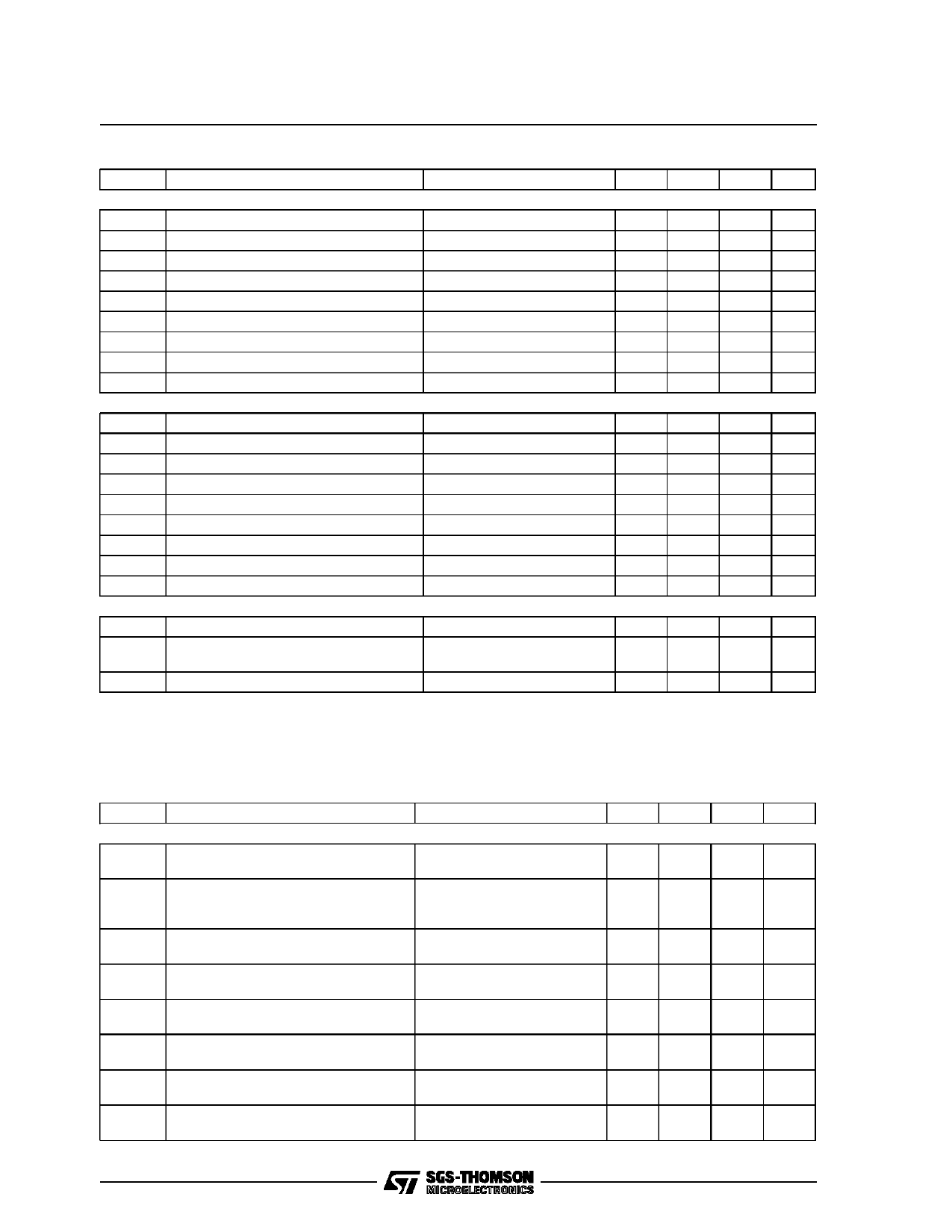
DC CHARACTERISTICS (continued)
Symbol
Parameter
Test Conditions
Min.
POWER DISSIPATION All measurements made at fDCLK = 2.048MHz, outputs unloaded
ICC1 VCC Operating Current
IBB1 VBB Operating Current
ICC0 VCC Power Down Current
PDN ≤ VIL ; after 10µs
IBB0 VBB Power Down Current
PDN ≤ VIL ; after 10µs
ICCS VCC Standby Current
FSX, FSR ≤ VIL ; after 30ms
IBBS VBB Standby Current
FSX, FSR ≤ VIL ; after 30ms
PD1 Operating Power Dissipation
PD0 Power Down Dissipation
PST Standby Power Dissipation
PDN ≤ VIL ; after 10µs
FSX, FSR ≤ VIL ; after 30ms
ANALOG INTERFACE, RECEIVE FILTER DRIVER AMPLIFIER STAGE
IBX1 Input Leakage Current, VFXI+, VFXI-
-2.17V ≤ VIN ≤ 2.17V
RIXI Input Resistance, VFXI+, VFXI-
10
VOSXI Input Offset Voltage, VFXI+, VFXI-
CMRR Common Mode Rejection, VFXI+, VFXI- -2.17V ≤ VIN ≤ 2.17V
55
AVOL DC Open Loop Voltage Gain, GSX
RL = 10K
5000
fC
Open Loop Unity Gain Bandwidth, GSX
VOXI Output Voltage Swing GSX
RL ≥ 10kΩ
– 2.17
CLXI Load Capacitance, GSX
RLXI Minimum Load Resistance, GSX
10
ANALOG INTERFACE, RECEIVE FILTER DRIVER AMPLIFIER STAGE
RORA Output Resistance, PWRO+, PWRO-
VOSRA Single-ended Output DC Offset,
PWRO+, PWRO-
Relative to GRDA
-150
CLRA Load Capacitance, PWRO+, PWRO-
Typ.
6
6
40
40
300
40
60
0.4
1.7
20.000
1
1
75
Max
10
9
300
300
600
300
100
3
5
100
25
2.17
50
150
100
Unit
mA
mA
µA
µA
µA
µA
mW
mW
mW
nA
MΩ
mV
dB
MHz
V
pF
kΩ
Ω
mV
pF
AC CHARACTERISTICS - TRANSMISSION PARAMETERS
Unless otherwie noted, the analog input is a 0dBm0, 1020Hz sine wave1. Input amplifier is set for unity
gain, noninverting. The digital inputs is a PCM bit stream generated by passing a 0dBm0, 1020Hz sine
wave through an ideal encoder. Receive output is measured single ended, maximum gain configuration2.
All output levels are (sin X)/X corrected.
Symbol
Parameter
GAIN AND DYNAMIC RANGE
EmW Encoder Milliwatt Response
(transmit gain tolerance)
EmWTS EmW Variation with Temperature and
Supplies
DmW
DmWTS
0TLP1X
0TLP2X
0TLP1R
0TLP2R
Digital Milliwatt Response
(receive gain tolerance)
DmW Variation with Temperature and
Supplies
Zero Transmission Level Point
Transmit Channel (0dBm0) µ-law
Zero Transmission Level Point
Transmit Channel (0dBm0) A-law
Zero Receive Level Point
Receive Channel (0dBm0) µ-law
Zero Transmission Level Point
Transmit Channel (0dBm0)) A-law
Test Conditions
Tamb = 25°C, VBB = – 5V,
VCC = + 5V
± 5% Supplies, 0 to 70°C
Relative to Nominal
Conditions
Tamb = 25°C ; VBB = – 5V,
VCC = + 5V
± 5%, 0 to 70°C
Referenced to 600Ω
Referenced to 900Ω
Referenced to 600Ω
Referenced to 900Ω
Referenced to 600Ω
Referenced to 900Ω
Referenced to 600Ω
Referenced to 900Ω
Min. Typ. Max. Unit
-0.15 ± 0.04 +0.15 dBm0
-0.12
+0.12 dB
-0.15 ± 0.04 +0.15 dBm0
-0.08
+0.08 dB
+ 2.76
+ 1.00
+ 2.79
+ 1.03
+ 5.76
+ 4.00
+ 5.79
+ 4.03
dBm
dBm
dBm
dBm
dBm
dBm
dBm
dBm
8/17
Share Link: 