M5913B1 データシートの表示(PDF) - STMicroelectronics
部品番号
コンポーネント説明
メーカー
M5913B1 Datasheet PDF : 17 Pages
| |||
M5913
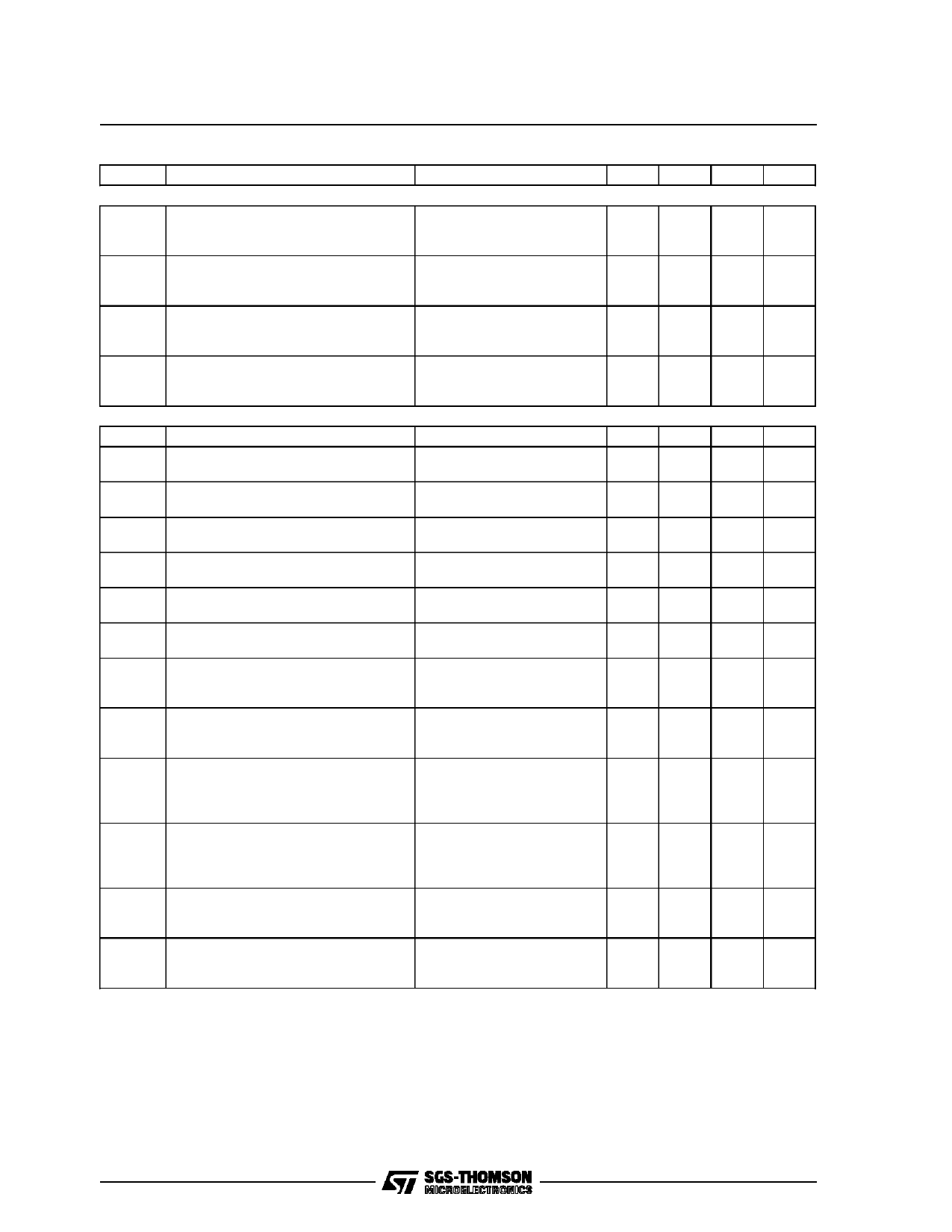
AC CHARACTERISTICS (continued)
Symbol
Parameter
GAIN TRACKING Reference Level = – 10dBm0
GT1X Transmit Gain Tracking Error
Sinusoidal Input; µ-law
GT2X Transmit Gain Tracking Error
Sinusoidal Input; A-law
GT1R Receive Gain Tracking Error
Sinusoidal Input; µ-law
GT2R Receive Gain Tracking Error
Sinusoidal Input; A-law
NOISE
NXC1
NXC2
NXP
NRC1
NRC2
NRP
NSF
PSRR1
Transmit Noise, C-message Weighted
Transmit Noise, C-message
Weighted with Eighth Bit Signaling
Transmit Noise, Psophometrically
Weighted
Receive Noise, C-message Weighted:
Quiet Code
Receive Noise, C-message Weighted:
Sign Bit Toggle
Receive Noise, Psophometrically
Weighted
Single Frequency NOISE End to End
Measurement
VCC Power Supply Rejection, Transmit
Channel
PSRR2 VBB Power Supply Rejection, Transmit
Channel
PSRR3 VCC Power Supply Rejection, Receive
Channel
PSRR4 VBB Power Supply, Rejection Receive
Channel
CTTR
Crosstalk, Transmit to Receive,
Single Ended Outputs
CTRT Crosstalk, Receive to Transmit,
Single Ended Outputs
Test Conditions
+ 3 to – 40dBm0
– 40 to – 50dBm0
– 50 to – 55dBm0
+ 3 to – 40dBm0
– 40 to – 50dBm0
– 50 to – 55dBm0
+ 3 to – 40dBm0
– 40 to – 50dBm0
– 50 to – 55dBm0
+ 3 to – 40dBm0
– 40 to – 50dBm0
– 50 to – 55dBm0
VFXI+ = GRDA, VFXI– = GSX
VFXI+ = GRDA, VFXI– = GSX
6 th Frame Signaling
VFXI+ = GRDA, VFXI– = GSX
DR = 11111111 Measure at
PWRO+
Input to DR is 0 code with
Sign Bit Toggle at 1KHz Rate
DR = Lowest Positive Decode
Level
CCITT G.712.4.2
Idle Channel ; 200mV P-P
Signal on Supply ; 0 to
50kHz, Measure at DX
Idle Channel ; 200mV P-P
Signal on Supply ; 0 to
50kHz, Measure at DX
Idle Channel ; 200mV P-P
Signal on Supply ; Measure
Narrow Band at PWRO+
Single Ended, 0 to 50kHz
Idle Channel ; 200mV P-P
Signal on Supply ; Measure
Narrow Band at PWRO+
Single Ended, 0 to 50kHz
VFXI+ = 0dBm0, 1.02kHz,
DR = Lowest Positive Decode
Level, Measure at PWRO+
DB = 0dBm0, 1.02kHz,
VFXI+ = GRDA, Measure at
DX
Min. Typ. Max. Unit
± 0.2 dB
± 0.4 dB
± 1.0 dB
± 0.2 dB
± 0.4 dB
± 1.0 dB
± 0.2 dB
± 0.4 dB
± 1.0 dB
± 0.2 dB
± 0.4 dB
± 1.0 dB
0
13 dBrnc0
13
18 dBrnc0
(note 3) – 80 dBrnc0
1
9 dBrnc0
1
10 dBm0p
-90 – 81 dB0p
– 50 dBm0
– 40
dB
– 40
dB
– 40
dB
– 40
dB
– 80 dB
– 80 dB
Notes:
1. 0dBm0 is defined as the zero reference point of the channel under test (0TLP). This corresponds to an analog signal input of 1.064 Vrms
or an output of 1.503 Vrmst (µLaw) dual 1.068 Vrmst or a output 1.516 Vrmst (A-Law)
2. Unity gain input amplifier : GSX is connected to VFXI, Signal input VFXI+; Maximum gain output amplifier: GSR is connected to PWRO,
output to PWRO+.
3. Noise free: DX PCM Code stable at 01010101.
9/17
Share Link: 