M59BW102N データシートの表示(PDF) - STMicroelectronics
部品番号
コンポーネント説明
メーカー
M59BW102N Datasheet PDF : 24 Pages
| |||
M59BW102
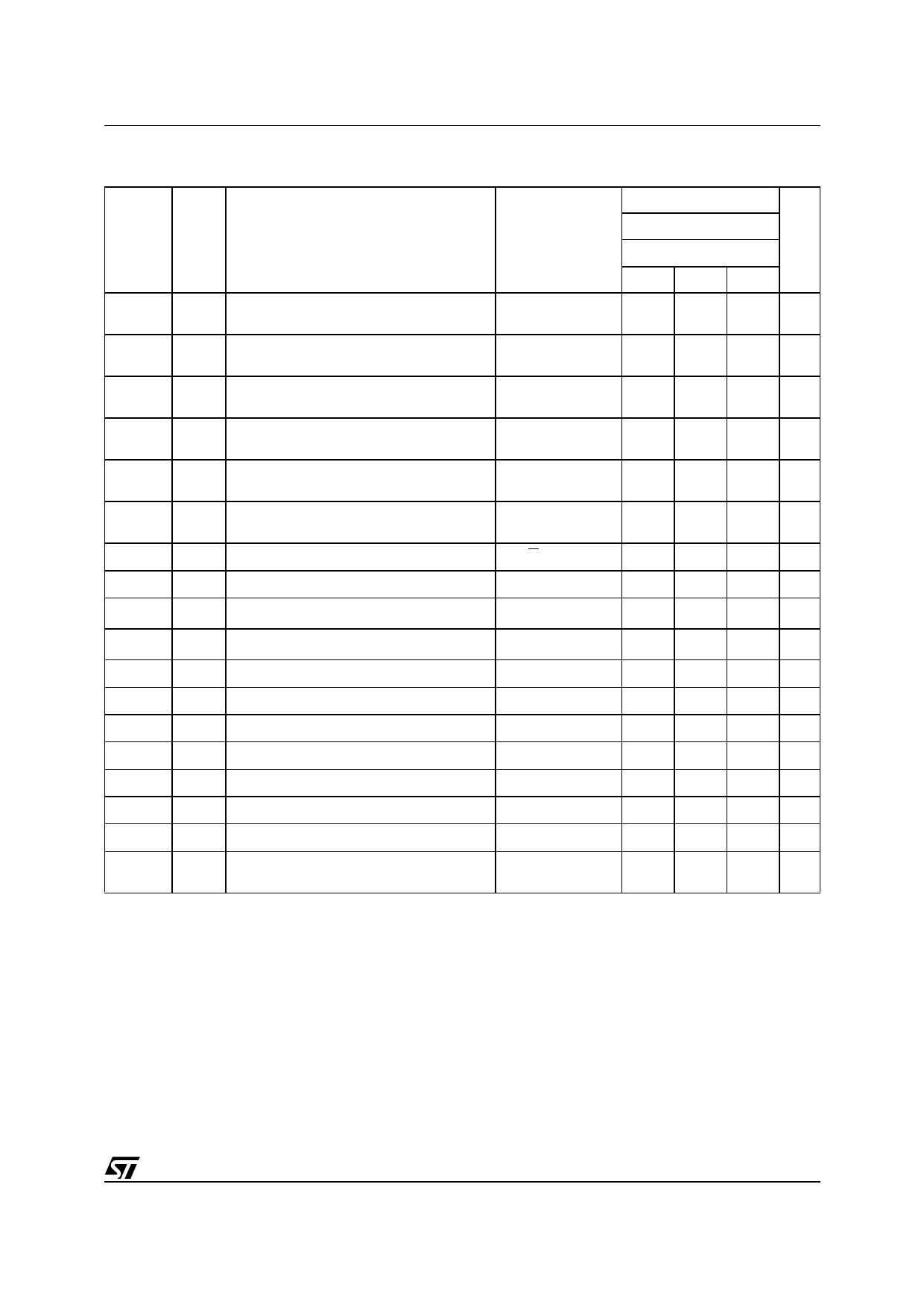
Table 13. Random Read Mode AC Characteristics
(TA = 0 to 70°C)
M59BW102
Symbol Alt
Parameter
Test Condition
25
VCC = 3.0V to 3.6V
Min Typ Max
tALHALL
tALW
Address Latch Enable High to Address
Latch Enable Low
ALE = Pulse
10
tELALL
tE
Chip Enable Low to Address Latch Enable
Low
10
tAXALL
tAS
Address Transition to Address Latch
Enable Low
6
tEHALH
tELV
Chip Enable High to Address Latch Enable
High
3
tALLGL
tAG
Address Latch Enable Low to Output
Enable Low
7.5
tGHALH
tQP
Output Enable High to Address Latch
Enable High
0
tGHGL tGW Output Enable High to Output Enable Low
G = Pulse
14
tGLGH
tGL Output Enable Low to Output Enable High
48
tGLQV (1) tGACC Output Enable Low to Output Valid
30
tELQV (1) tEACC Chip Enable Low to Output Valid
55
tGHEL
tGE Output Enable High to Chip Enable Low
–2
tEHQZ tEDF Chip Enable High to Output Hi-Z
12
tALHQZ tADF Address Latch Enable High to Output Hi-Z
20
tQVGH
tQV Output Valid to Output Enable High
10
tGHEH
tGE Output Enable High to Chip Enable High
0
tELGL
tEGL Chip Enable Low to Output Enable Low
13
tEHQV
Chip Enable High to Data Hold
0
tALLAX
Address Latch Enable Low to Address
Transition
30
Note: 1. This timing refers to a Load Capacitance (CL) of 30pF. If CL is higher, add 1ns for each extra 10pF.
Unit
ns
ns
ns
ns
ns
ns
ns
ns
ns
ns
ns
ns
ns
ns
ns
ns
ns
ns
11/24
Share Link: 