M59BW102N データシートの表示(PDF) - STMicroelectronics
部品番号
コンポーネント説明
メーカー
M59BW102N Datasheet PDF : 24 Pages
| |||
M59BW102
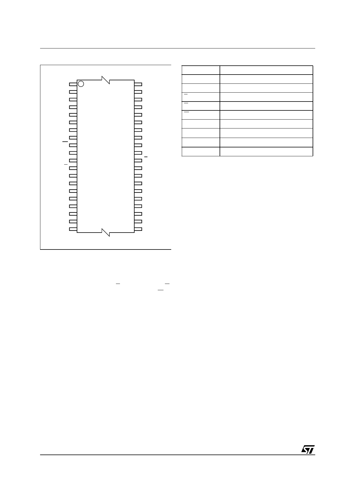
Figure 2. TSOP Connections
A9
A10
A11
A12
A13
A14
A15
ALE
W
VCC
NC
E
DQ15
DQ14
DQ13
DQ12
DQ11
DQ10
DQ9
DQ8
1
40
10 M59BW102 31
11
30
20
21
AI02764B
VSS
A8
A7
A6
A5
A4
A3
A2
A1
A0
G
DQ0
DQ1
DQ2
DQ3
DQ4
DQ5
DQ6
DQ7
VSS
Organization
The M59BW102 is organized as 64K x16 bits. The
memory uses the address inputs A0-A15 and the
Data Inputs/Outputs DQ0-DQ15. Memory control
is provided by Chip Enable E, Output Enable G,
Address Latch Enable ALE and Write Enable W in-
puts.
Erase and Program operations are controlled by
an internal Program/Erase Controller (P/E.C.).
Status Register data output on DQ7 provides a
Data Polling signal, and DQ6 and DQ2 provide
Toggle signals to indicate the state of the P/E.C
operations.
Bus Operations
The following operations can be performed using
the appropriate bus cycles: Read (Array, Electron-
ic Signature), Write command, Output Disable,
Standby. See Tables 3 and 4.
Table 1. Signal Names
A0-A15
Address Inputs
DQ0-DQ7
Data Inputs/Outputs, Command Inputs
DQ8-DQ15 Data Inputs/Outputs
E
Chip Enable
G
Output Enable
W
Write Enable
ALE
Address Latch Enable
VCC
Supply Voltage
VSS
Ground
NC
Not Connected Internally
Command Interface
Instructions, made up of commands written in cy-
cles, can be given to the Program/Erase Controller
through a Command Interface (C.I.). For added
data protection, program or erase execution starts
after 4 or 6 cycles. The first, second, fourth and
fifth cycles are used to input Coded cycles to the
C.I. This Coded sequence is the same for all Pro-
gram/Erase Controller instructions. The ’Com-
mand’ itself and its confirmation, when applicable,
are given on the third, fourth or sixth cycles. Any
incorrect command or any improper command se-
quence will reset the device to Read Array mode.
Instructions
Four instructions are defined to perform Read Ar-
ray, Auto Select (to read the Electronic Signature),
Program, Chip Erase. The internal P/E.C. auto-
matically handles all timing and verification of the
Program and Erase operations. The Status Regis-
ter Data Polling, Toggle and Error bits may be read
at any time, during programming or erase, to mon-
itor the progress of the operation.
Instructions are composed of up to six cycles. The
first two cycles input a Coded sequence to the
Command Interface which is common to all in-
structions (see Table 7). The third cycle inputs the
instruction set-up command. Subsequent cycles
output the addressed data or Electronic Signature
for Read operations. In order to give additional
data protection, the instructions for Program and
Chip Erase require further command inputs. For a
Program instruction, the fourth command cycle in-
puts the address and data to be programmed. For
an Erase instruction, the fourth and fifth cycles in-
put a further Coded sequence before the com-
mand confirmation on the sixth cycle.
2/24
Share Link: 