M59BW102N データシートの表示(PDF) - STMicroelectronics
部品番号
コンポーネント説明
メーカー
M59BW102N Datasheet PDF : 24 Pages
| |||
M59BW102
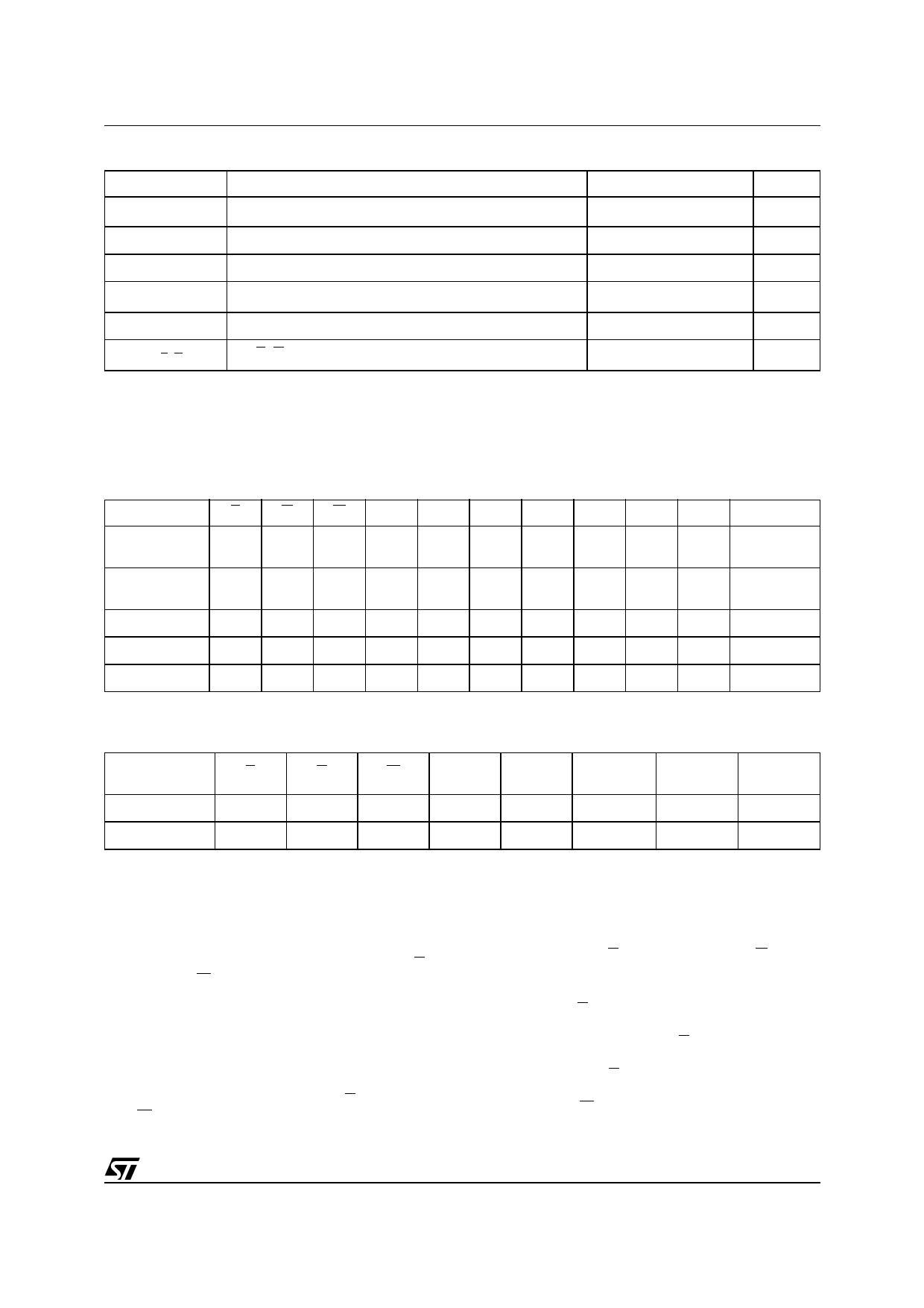
Table 2. Absolute Maximum Ratings (1)
Symbol
Parameter
Value
Unit
TA
Ambient Operating Temperature
0 to 70
°C
TBIAS
Temperature Under Bias
–50 to 125
°C
TSTG
Storage Temperature
–65 to 150
°C
VIO (2)
Input or Output Voltage
–0.6 to 5
V
VCC
Supply Voltage
–0.6 to 5
V
V(A9, E, G) (2)
A9, E, G Voltage
–0.6 to 13.5
V
Note: 1. Except for the rating "Operating Temperature Range", stresses above those listed in the Table "Absolute Maximum Ratings" may
cause permanent damage to the device. These are stress ratings only and operation of the device at these or any other conditions
above those indicated in the Operating sections of this specification is not implied. Exposure to Absolute Maximum Rating condi-
tions for extended periods may affect device reliability. Refer also to the STMicroelectronics SURE Program and other relevant qual-
ity documents.
2. Minimum Voltage may undershoot to –2V during transition and for less than 20ns.
Table 3. User Bus Operations (1))
Operation
E
G
W ALE A0
A1
A6
A9 A12 A15 DQ15-DQ0
Non Linear
Access Mode
VIL
VIL
VIH Pulse X
X
X
X
X
X Data Output
Linear Access
Cycle
VIL
Rising
Edge
VIH
VIL
X
X
X
X
X
X Data Output
Write Word
VIL
VIH
VIL
VIH
A0
A1
A6
A9 A12 A15 Data Input
Output Disable VIL
VIH
VIH
VIH
X
X
X
X
X
X
Hi-Z
Standby
VIH
X
X
X
X
X
X
X
X
X
Hi-Z
Note: 1. X = VIL or VIH.
Table 4. Read Electronic Signature (following AS instruction or with A9 = VID)
Code
E
G
W
A0
A1
Other
Address
DQ15-DQ8
DQ7-DQ0
Manufact. Code
VIL
VIL
VIH
VIL
VIL
Don't Care
00h
20h
Device Code
VIL
VIL
VIH
VIH
VIL
Don't Care
00h
C1h
SIGNAL DESCRIPTIONS
See Figure 1 and Table 1.
Address Inputs (A0-A15). The address inputs
for the memory array are latched during a write op-
eration on the falling edge of Chip Enable E or
Write Enable W. When A9 is raised to VID, either a
Read Electronic Signature Manufacturer or Device
Code is enabled depending on the combination of
levels on A0 and A1.
Data Inputs/Outputs (DQ0-DQ15). The input is
data to be programmed in the memory array or a
command to be written to the C.I. Both are latched
on the rising edge of Chip Enable E or Write En-
able W. The output is data from the Memory Array,
the Electronic Signature Manufacturer or Device
codes, the Status register Data Polling bit DQ7,
the Toggle Bits DQ6 and DQ2, the Error bit DQ5
or the Erase Timer bit DQ3. Outputs are valid
when Chip Enable E and Output Enable G are ac-
tive. The output is high impedance when the chip
is deselected or the outputs are disabled.
Chip Enable (E). The Chip Enable input acti-
vates the memory control logic, input buffers, de-
coders and sense amplifiers. E High deselects the
memory and reduces the power consumption to
the standby level. E can also be used to control
writing to the command register and to the memo-
ry array, while W remains at a low level.
3/24
Share Link: 