M59BW102N データシートの表示(PDF) - STMicroelectronics
部品番号
コンポーネント説明
メーカー
M59BW102N Datasheet PDF : 24 Pages
| |||
M59BW102
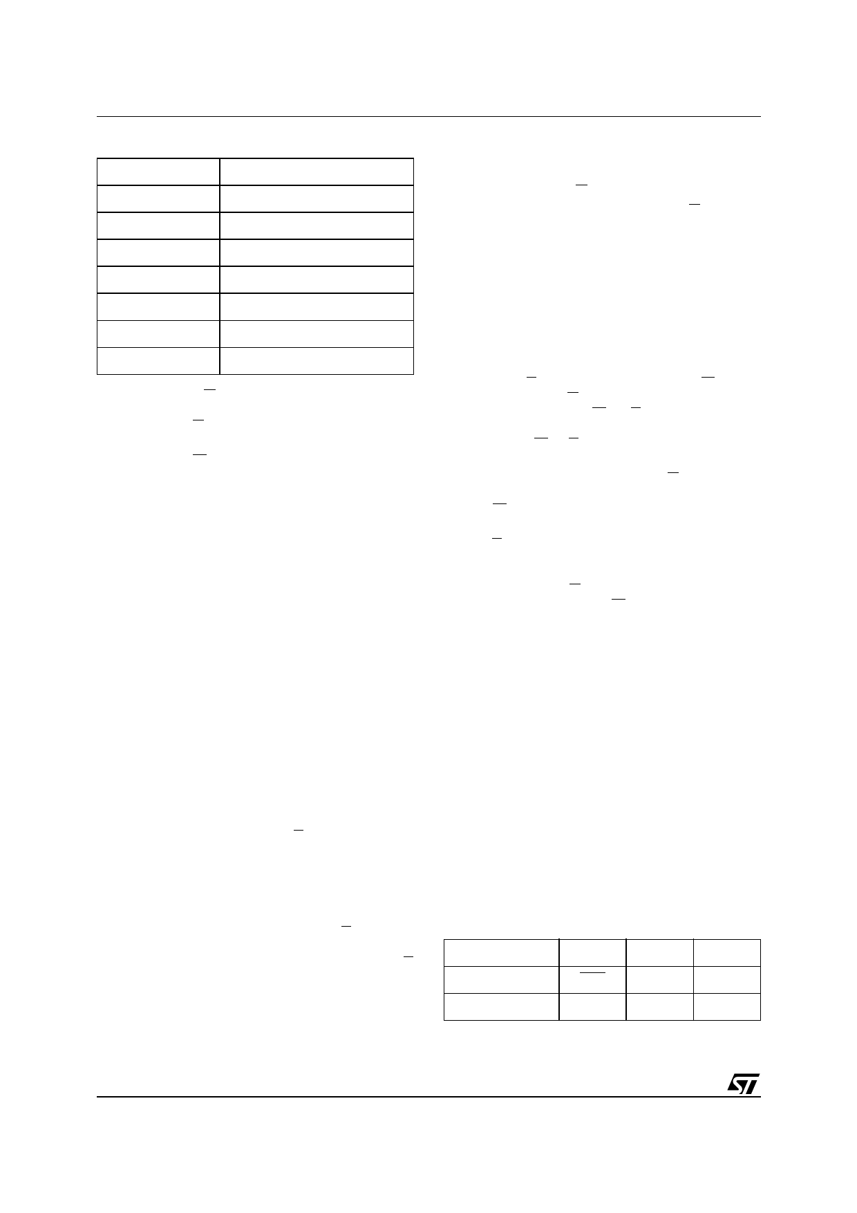
Table 5. Commands
Hex Code
Command
00h
Invalid/Reserved
10h
Chip Erase Confirm
20h
Reserved
80h
Set-up Erase
90h
Read Electronic Signature
A0h
Program
F0h
Read Array/Reset
Output Enable (G). The Output Enable gates the
outputs through the data buffers during a read op-
eration. When G and ALE are both High the out-
puts are High impedance.
Write Enable (W). This input controls writing to
the Command Register and Address and Data
latches.
Address Latch Enable (ALE). This input con-
trols the latching of address for reading. When
pulsed, the device operates in the random or non
linear access mode.
VCC Supply Voltage. The power supply for all
operations (Read, Program and Erase).
VSS Ground. VSS is the reference for all voltage
measurements.
DEVICE OPERATIONS
See Tables 3 and 4.
Read (Non Linear Access Mode and Linear Ac-
cess Cycle). The device is internally organized in
two memory banks (named Even and Odd bank).
A0 address bit is asserted as "priority" bit, so that
when A0 = 0 the even bank is the current memory
array under selection and the odd bank is masked.
When A0 = 1 the odd bank is the current array un-
der selection and even bank is masked.
To begin a random (or Non Linear) access mode
(NLA), ALE is pulsed high and E is asserted low.
Two internal 15 bit counters store the current ad-
dress for the odd and even banks and increment
alternatively, under the priority bit control, during
each subsequent cycle called sequential (or Lin-
ear) address cycle (LA). The linear cycle (LA) can
be terminated if a new NLA starts or if E is assert-
ed high, putting the device in stand-by mode. In
this last case the linear cycle can be resumed if E
is asserted low again and ALE is low.
During the LA mode all the memory can be swept,
as there is no physical limits to the linear access
output. When the last address of the memory is
reached by the counters they start again from the
first memory address and continue. The
M59BW102 will provide data output during the LA
cycle determined by G signal.
Each time ALE signal is pulsed and G signal is
High, while the current address is loaded into the
counters, the output buffers are put in Hi-Z condi-
tion and remain in this condition until the first new
valid data comes. The M59BW102 operation in LA
and NLA modes is explained in Figure 3 and the
block diagram is shown in Figure 4.
Write. Write operations are used to give Instruc-
tion Commands to the memory or to latch input
data to be programmed. A write operation is initi-
ated when Address Latch Enable (ALE) is high,
Chip Enable E is Low and Write Enable W is Low
with Output Enable G High. Addresses are latched
on the falling edge of W or E whichever occurs
last. Commands and Input Data are latched on the
rising edge of W or E whichever occurs first.
Output Disable. The data outputs are high im-
pedance when the Output Enable G and the Ad-
dress Latch Enable (ALE) are both High with Write
Enable W High.
Standby. The memory is in standby when Chip
Enable E is High and the P/E.C. is idle. The power
consumption is reduced to the standby level and
the outputs are high impedance, independent of
the Output Enable G, the Address Latch Enable
(ALE) or the Write Enable W inputs.
Electronic Signature. Two codes identifying the
manufacturer and the device can be read from the
memory. The manufacturer’s code for
STMicroelectronics is 20h, the device code is C1h.
These codes allow programming equipment or ap-
plications to automatically match their interface to
the characteristics of the M59BW102. The Elec-
tronic Signature is output by a Read operation
when the voltage applied to A9 is at VID and ad-
dress inputs A1 is Low. The manufacturer code is
output when the Address input A0 is Low and the
device code when this input is High. Other Ad-
dress inputs are ignored. The codes are output on
DQ0-DQ7.
The Electronic Signature can also be read, without
raising A9 to VID, by giving the memory the In-
struction AS. The codes are output on DQ0-DQ7
with DQ8-DQ15 at 00h.
Table 6. Polling and Toggle Bits
Mode
DQ7
DQ6
Program
DQ7
Toggle
Erase
0
Toggle
DQ2
1
Toggle
4/24
Share Link: 