M59BW102N データシートの表示(PDF) - STMicroelectronics
部品番号
コンポーネント説明
メーカー
M59BW102N Datasheet PDF : 24 Pages
| |||
M59BW102
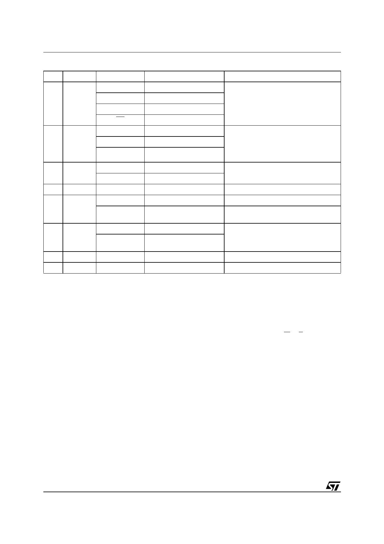
Table 8. Status Register Bits
DQ
Name
Logic Level
Definition
Note
7
Data
Polling
’1’
Erase Complete
’0’
Erase On-going
DQ
Program Complete
DQ
Program On-going
Indicates the P/E.C. status, check during
Program or Erase, and on completion before
checking bits DQ5 for Program or Erase
Success.
’-1-0-1-0-1-0-1-’ Erase or Program On-going Successive reads output complementary
6 Toggle Bit
DQ
Program Complete
data on DQ6 while Programming or Erase
operations are on-going. DQ6 remains at
’-1-1-1-1-1-1-1-’ Erase Complete
constant level when P/E.C. operations are
completed.
5 Error Bit
’1’
Program or Erase Error
This bit is set to ’1’ in the case of
’0’
Program or Erase On-going Programming or Erase failure.
4 Reserved
3
Erase
Time Bit
’1’
Erase Timeout Period Expired P/E.C. Erase operation has started.
’0’
Erase Timeout Period On-
going
’-1-0-1-0-1-0-1-’ Chip Erase
2 Toggle Bit
’1’
Program On-going or Erase
Complete
Indicates the erase status.
1 Reserved
0 Reserved
Note: Logic level ’1’ is High, ’0’ is Low. -0-1-0-0-0-1-1-1-0- represent bit value in successive Read operations.
Instructions
See Table 7.
Read/Reset (RD) Instruction. The Read/Reset
instruction consists of one write cycle giving the
command F0h. It can be optionally preceded by
the two Coded cycles. Subsequent read opera-
tions will read the memory array addressed and
output the data read. Read/Reset is not accepted
in Program/Erase operation unless a fail occurred.
Auto Select (AS) Instruction. This instruction
uses the two Coded cycles followed by one write
cycle giving the command 90h to address 555h for
command set-up. A subsequent read will output
the manufacturer code and the device code de-
pending on the levels of A0 and A1. The manufac-
turer code, 20h, is output when the addresses
lines A0 and A1 are Low, the device code, C1h is
output when A0 is High with A1 Low.
Program (PG) Instruction. This instruction uses
four write cycles. The Program command A0h is
written to address 555h on the third cycle after two
Coded cycles. A fourth write operation latches the
Address on the falling edge of W or E and the Data
to be written on the rising edge and starts the P/
E.C. Read operations output the Status Register
bits after the programming has started. Memory
programming is made only by writing ’0’ in place of
’1’. Status bits DQ6 and DQ7 determine if pro-
gramming is on-going and DQ5 allows verification
of any possible error.
Chip Erase (CE) Instruction. This instruction uses
six write cycles. The Set-up command 80h is writ-
8/24
Share Link: 