M59BW102N データシートの表示(PDF) - STMicroelectronics
部品番号
コンポーネント説明
メーカー
M59BW102N Datasheet PDF : 24 Pages
| |||
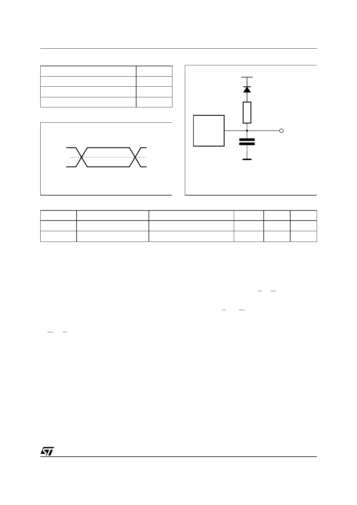
Table 9. AC Measurement Conditions
Load Capacitance (CL)
30pF
Input Rise and Fall Times
≤ 10ns
Input Pulse Voltages
0 to 3V
Input and Output Timing Ref. Voltages
1.5V
Figure 5. AC Testing Input Output Waveform
3V
1.5V
0V
AI01417
M59BW102
Figure 6. AC Testing Load Circuit
1.3V
1N914
DEVICE
UNDER
TEST
3.3kΩ
OUT
CL = 30pF
CL includes JIG capacitance
AI01119
Table 10. Capacitance (1) (TA = 25 °C, f = 1 MHz)
Symbol
Parameter
Test Condition
CIN
Input Capacitance
VIN = 0V
COUT
Output Capacitance
VOUT = 0V
Note: 1. Sampled only, not 100% tested.
Min
Max
Unit
6
pF
12
pF
ten to address 555h on the third cycle after the two
Coded cycles. The Chip Erase Confirm command
10h is similarly written on the sixth cycle after an-
other two Coded cycles. If the second command
given is not an erase confirm or if the Coded cy-
cles are wrong, the instruction aborts and the de-
vice is reset to Read Array. It is not necessary to
program the array with 0000h first as the P/E.C.
will automatically do this before erasing it to
FFFFh. Read operations after the sixth rising edge
of W or E output the Status Register bits. During
the execution of the erase by the P/E.C., Data
Polling bit DQ7 returns '0', then '1' on completion.
The Toggle bits DQ2 and DQ6 toggle during erase
operation and stop when erase is completed. After
completion the Status Register bit DQ5 returns '1'
if there has been an Erase Failure.
POWER SUPPLY
Power Up
The memory Command Interface is reset on pow-
er up to Read Array. Either E or W must be tied to
VIH during Power Up to allow maximum security
and the possibility to write a command on the first
rising edge of E and W. Any write cycle initiation is
blocked when VCC is below VLKO.
Supply Rails
Normal precautions must be taken for supply volt-
age decoupling; each device in a system should
have the VCC rail decoupled with a 0.1µF capacitor
close to the VCC and VSS pins. The PCB trace
widths should be sufficient to carry the VCC pro-
gram and erase currents required.
9/24
Share Link: 