M5M5256RV-55LL-I データシートの表示(PDF) - MITSUBISHI ELECTRIC
部品番号
コンポーネント説明
メーカー
M5M5256RV-55LL-I Datasheet PDF : 7 Pages
| |||
'97.4.7
MITSUBISHI LSIs
M5M5256DP,KP,FP,VP,RV -45LL-I,-55LL-I,-70LL-I,
-45XL-I,-55XL-I,-70XL-I
262144-BIT (32768-WORD BY 8-BIT) CMOS STATIC RAM
FUNCTION
The operation mode of the M5M5256DP,KP,FP,VP,RV is
determined by a combination of the device control inputs /S,
/W and /OE. Each mode is summarized in the function table.
A write cycle is executed whenever the low level /W
overlaps with the low level /S. The address must be set up
before the write cycle and must be stable during the entire
cycle. The data is latched into a cell on the trailing edge of
/W, /S, whichever occurs first, requiring the set-up and hold
time relative to these edge to be maintained. The output
enable /OE directly controls the output stage. Setting the
/OE at a high level,the output stage is in a high-impedance
state, and the data bus contention problem in the write cycle
is eliminated.
A read cycle is executed by setting /W at a high level and
/OE at a low level while /S are in an active state.
When setting /S at a high level, the chip is in a
non-selectable mode in which both reading and writing are
disabled. In this mode, the output stage is in a
high-impedance state, allowing OR-tie with other chips and
memory expansion by /S. The power supply current is
reduced as low as the stand-by current which is specified
as Icc3 or Icc4, and the memory data can be held at +2V
power supply, enabling battery back-up operation during
power failure or power-down operation in the non-selected
mode.
FUNCTION TABLE
/S /W /OE
Mode
H X X Non selection
L LX
Write
L HL
Read
L HH
DQ
High-impedance
DIN
DOUT
High-impedance
Icc
Stand-by
Active
Active
Active
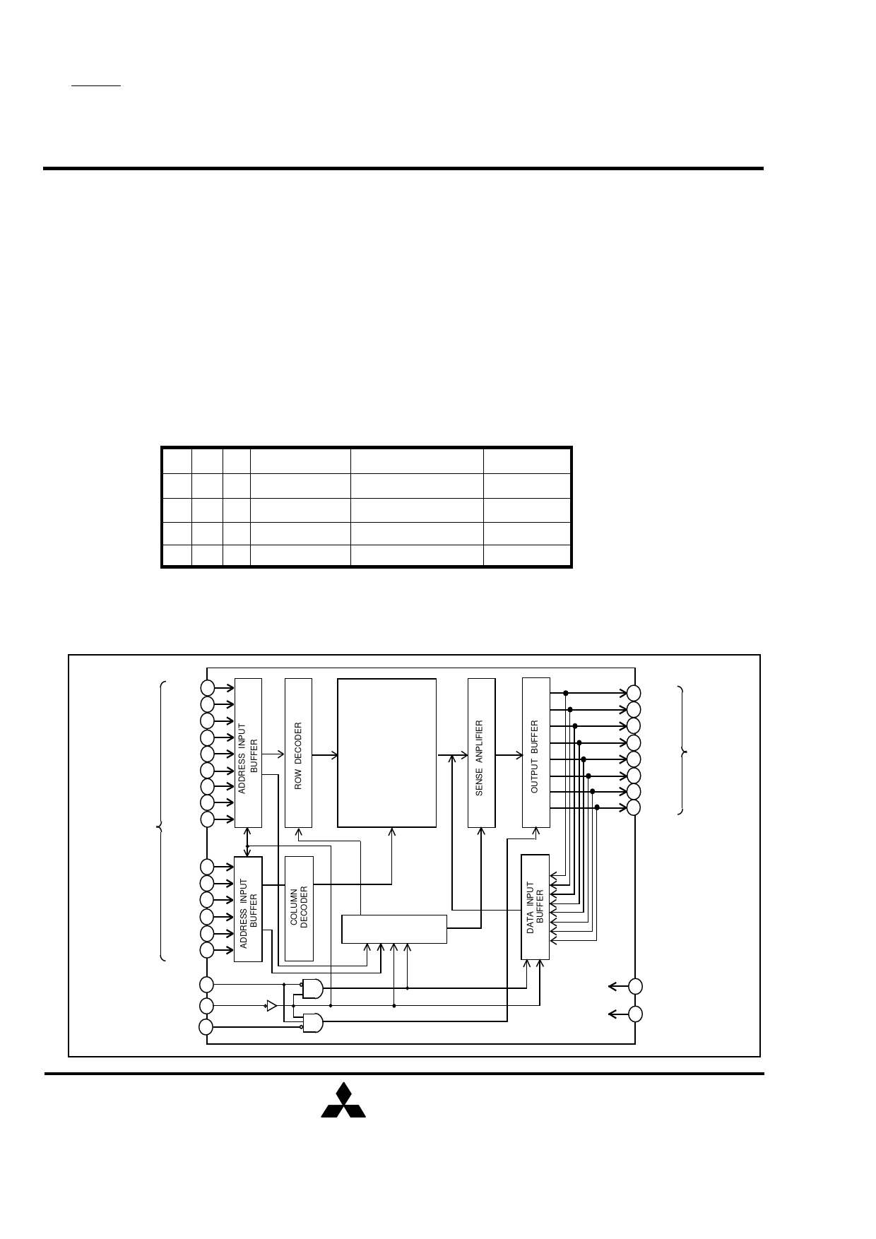
BLOCK DIAGRAM
ADDRESS
INPUT
A 8 25
A 13 26
A 14 1
A 12 22
A7 3
A6 4
A5 5
A4 6
A3 7
A2 8
A1 9
A 0 10
A 10 21
A 11 23
A 9 24
WRITE CONTROL
INPUT /W 27
CHIP SELECT
INPUT /S
20
OUTPUT ENABLE /OE 22
INPUT
32768 WORD
X 8BIT
(512 ROWS X
512 COLUMNS)
CLOCK
GENERATOR
MITSUBISHI
ELECTRIC
11 DQ1
12 DQ2
13 DQ3
15 DQ4
16 DQ5
17 DQ6
18 DQ7
19 DQ8
DATA I/O
28 VCC
(5V)
14 GND
(0V)
2
Share Link: 